-
3-hexylthiophene temp ScratchMode EFMAmplitude self-assembly LiBattery HighAspect OpticalWaveguide Polyaniline Aluminium_Oxide VinylAlcohol UnivCollegeLondon Temperature BoronNitride MagneticForceMicroscopy Galfenol PyroelectricDetector kelvin probe force microscopy single_layer DNAProtein Steps silicon_carbide AdhesionForce HanyangUniv Lattice IMT_Bucharest Switching Ferroelectric Growing Genetic HexagonalBN FM-KPFM OpticalModulator molecules FloppyDisk
Report image
If you found this image unacceptable, please let us know. We will review your report and take action if we determine this image is really unacceptable.
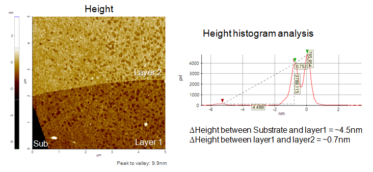
MoS2 Layers on SiO2

Scanning Conditions
- System: NX10
- Scan Mode: Non-contact
- Cantilever: AC160TS (k=26N/m, f=300kHz)
- Scan Size: 5μm×5μm
- Scan Rate: 1Hz
- Pixel Size: 256 × 256
- Scan Mode: Non-contact
- Cantilever: AC160TS (k=26N/m, f=300kHz)
- Scan Size: 5μm×5μm
- Scan Rate: 1Hz
- Pixel Size: 256 × 256
