-
TipBiasMode Mfm Litho I-VSpectroscopy lift_mode Silver fluoroalkane Sidewall Christmas Subhajjit Ni-FeAlloy DNAProtein Annealing Ucl Perovskite Memory Fujian AM_KPFM Reading YszSubstrate Spain Floppy Collagen temp Vac Dopped Styrene nanomechanical OrganicSemiconductor 2d_materials margarine Thermoplastic_polyurethane HfO2 neodymium_magnets Transparent
Report image
If you found this image unacceptable, please let us know. We will review your report and take action if we determine this image is really unacceptable.
Polymer patterns on Si (1/2)
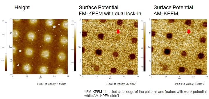
Scanning Conditions
- System: NX10
- Scan Mode: KPFM
- Cantilever: NSC36Cr-Au (k=1N/m, f=90kHz)
- Scan Size: 10μm×10μm
- Scan Rate: 0.2Hz
- Pixel: 512×256