-
LightEmission SKPM Polystyrene Bio FloppyDisk Magnetostrictive IVSpectroscopy Piranha Stiffness ElectrostaticForceMicroscopy Potential Phenanthrene Chrome LithiumNiobate HafniumDioxide Corrosion PUR Conductance MfmAmplitude Electronics CuFoil Wildtype Thermal BismuthFerrite ito_film SICM Al2O3 PS_LDPE AEAPDES PtfeFilter Tin disulfide FailureAnlaysis Wafer Optic HardDiskMedia
Report image
If you found this image unacceptable, please let us know. We will review your report and take action if we determine this image is really unacceptable.
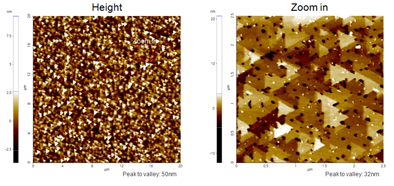
LiNbO3 wafer

Scanning Conditions
- System: NX10
- Scan Mode: Non-contact
- Cantilever: AC55TS (k=85N/m, f=1600kHz)
- Scan Size:20μm×20μm, 2.5μm×2.5μm
- Scan Rate: 5Hz, 10Hz
- Pixel: 512×512, 256×256
- Scan Mode: Non-contact
- Cantilever: AC55TS (k=85N/m, f=1600kHz)
- Scan Size:20μm×20μm, 2.5μm×2.5μm
- Scan Rate: 5Hz, 10Hz
- Pixel: 512×512, 256×256
