-
Holes CeramicCapacitor HighResolution FrictionForce EFMAmplitude temp_control nanobar MoirePattern PolymerPatterns Sulfur BaTiO3 SSRM Melt HACrystal Gold Pinpoint #EC MfmPhase Au111 ThermalDetectors norganic 3-hexylthiophene HighAcpectRatio Platinum rubber thermal_property Wildtype Korea FailureAnalysis CeNSE_IISc IcelandSpar Solar Etch SiliconCrystal PDMS
Report image
If you found this image unacceptable, please let us know. We will review your report and take action if we determine this image is really unacceptable.
Multi-layer necking device defect
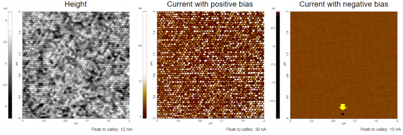
Scanning Conditions
- System : NX-Wafer
- Scan Mode: C-AFM
- Scan Rate : 2Hz
- Scan Size : 2μm×2μm
- Pixel Size : 512×256
- Cantilever : AD-2.8-AS (k=2.8N/m, f=75kHz)