-
MultiLayerCeramicCapacitor TungstenThinFilmDeposition Wang ForceVolume Vacuum Thermoplastic_polyurethane fluoroalkane Butterfly NUS Litho plastics Silver Hair Aluminium_Oxide Singapore Adhesion Pore strontiu_titanate EFMAmplitude Insulator norganic StainlessSteel #Materials Mosfet Phosphide HexagonalBoronNitride LiIonBattery Current LiquidImaging Polyvinylidene CVD PDMS ChemicalCompound Ni81Fe19 Lattice
Report image
If you found this image unacceptable, please let us know. We will review your report and take action if we determine this image is really unacceptable.
Monolayer Graphene on PDMS Surface
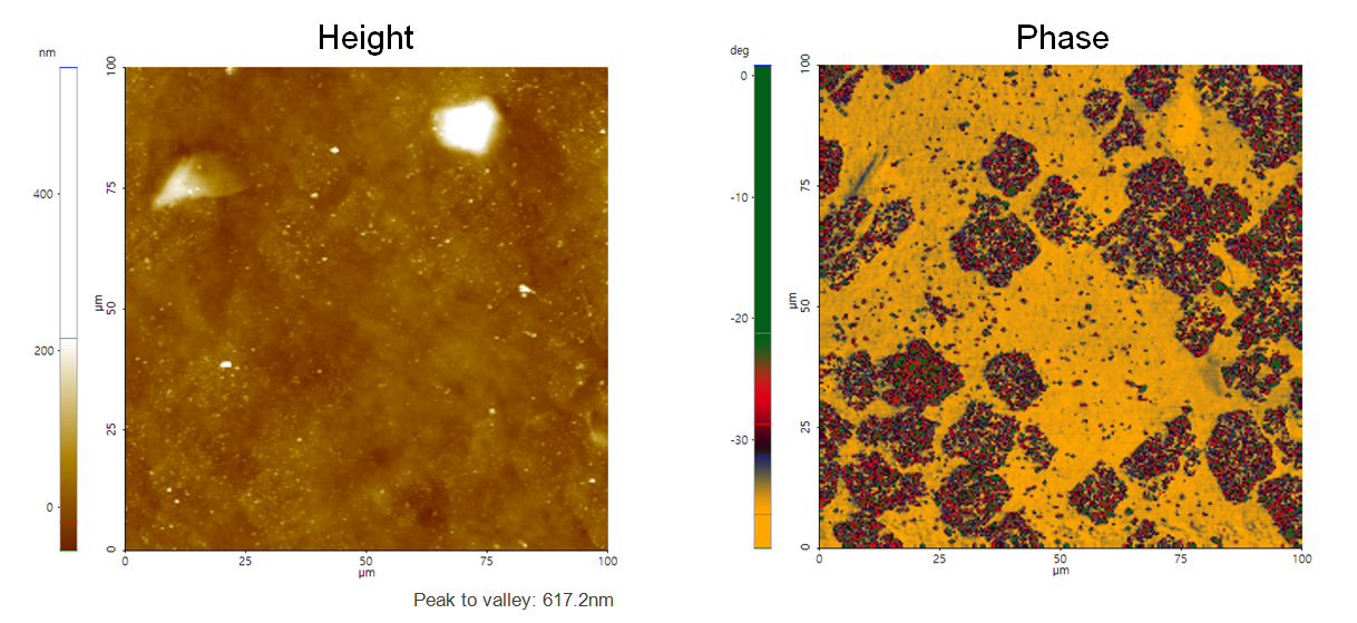
Monolayer Graphene grown on Cu foil using CVD process is transferred on to PDMS substrate.
Scanning Conditions
- System: NX20
- Scan Mode: Tapping
- Cantilever: Access-NC (k=113N/m, f=330kHz)
- Scan Size: 100μm×100μm
- Scan Rate: 0.6Hz
- Pixel Size: 256 × 256
- Scan Mode: Tapping
- Cantilever: Access-NC (k=113N/m, f=330kHz)
- Scan Size: 100μm×100μm
- Scan Rate: 0.6Hz
- Pixel Size: 256 × 256