-
FrictionalForceMicroscopy Conductivity Hair Ni-FeAlloy Pzt PFM MBE Temasek_Lab CntFilm MLCC LDPE temp_control Sperm DiffractiveOpticalElements Ferrite epitaxy Deposition PinPointMode Multiferroic_materials Protein LateralForceMicroscopy Force-distance ThermalProperties InLiquid Treatment FrictionalForce CaMnO3 PolyvinylideneFluoride ContactMode MonoLayer Foil F14H20 OpticalModulator Silicon FM-KPFM
Report image
If you found this image unacceptable, please let us know. We will review your report and take action if we determine this image is really unacceptable.
MoS2 Layers on SiO2
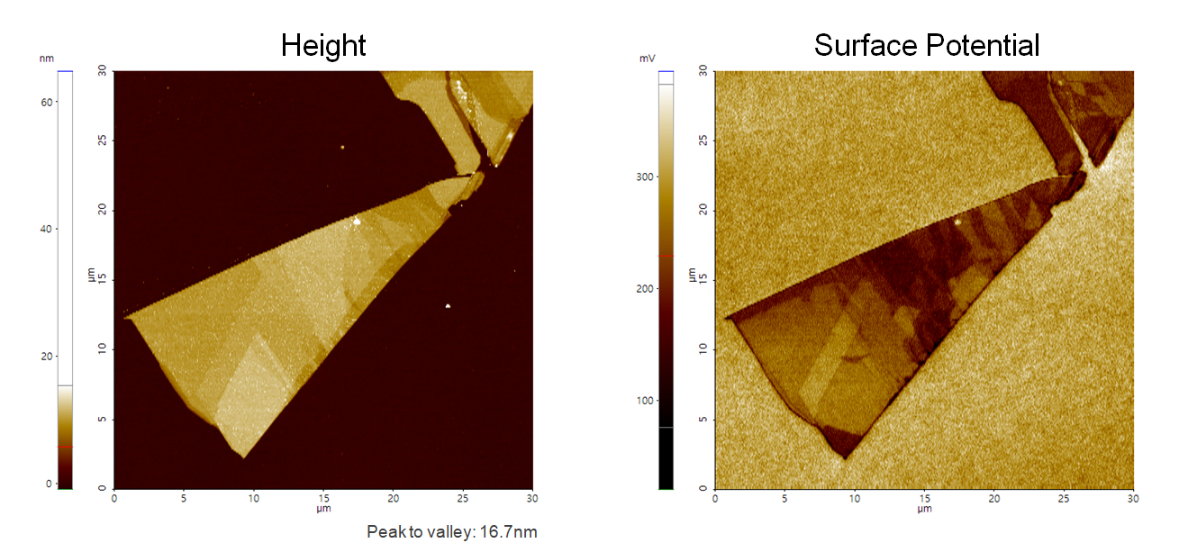
A few layers of MoS2 on SiO2
Scanning Conditions
- System: NX10
- Scan Mode: AM-KPFM
- Cantilever: NSC36Cr-Au B (k=2N/m, f=130kHz)
- Scan Size: 30μm×30μm
- Scan Rate: 0.3Hz
- Pixel Size: 512 × 256
- Scan Mode: AM-KPFM
- Cantilever: NSC36Cr-Au B (k=2N/m, f=130kHz)
- Scan Size: 30μm×30μm
- Scan Rate: 0.3Hz
- Pixel Size: 512 × 256