-
TiO2 SThM DentalProsthesis Butterfly DIWafer Cobalt-dopedIronOxide AEAPDES Cancer LateralForceMicroscopy PrCurve ForceVolume StrontiumTitanate Ptfe Blood Pore IMT_Bucharest Ni-FeAlloy SiliconOxide Nanopattern BreastCancerCell sputter Annealing CrystalGrowing INSP molecules Bio Thermoplastic_polyurethane block_copolymer HexagonalBoronNitride StainlessSteel Copolymer BoronNitride GaN GaAs Bismuth
Report image
If you found this image unacceptable, please let us know. We will review your report and take action if we determine this image is really unacceptable.
ITO Film Sputter Deposited onto Silicon
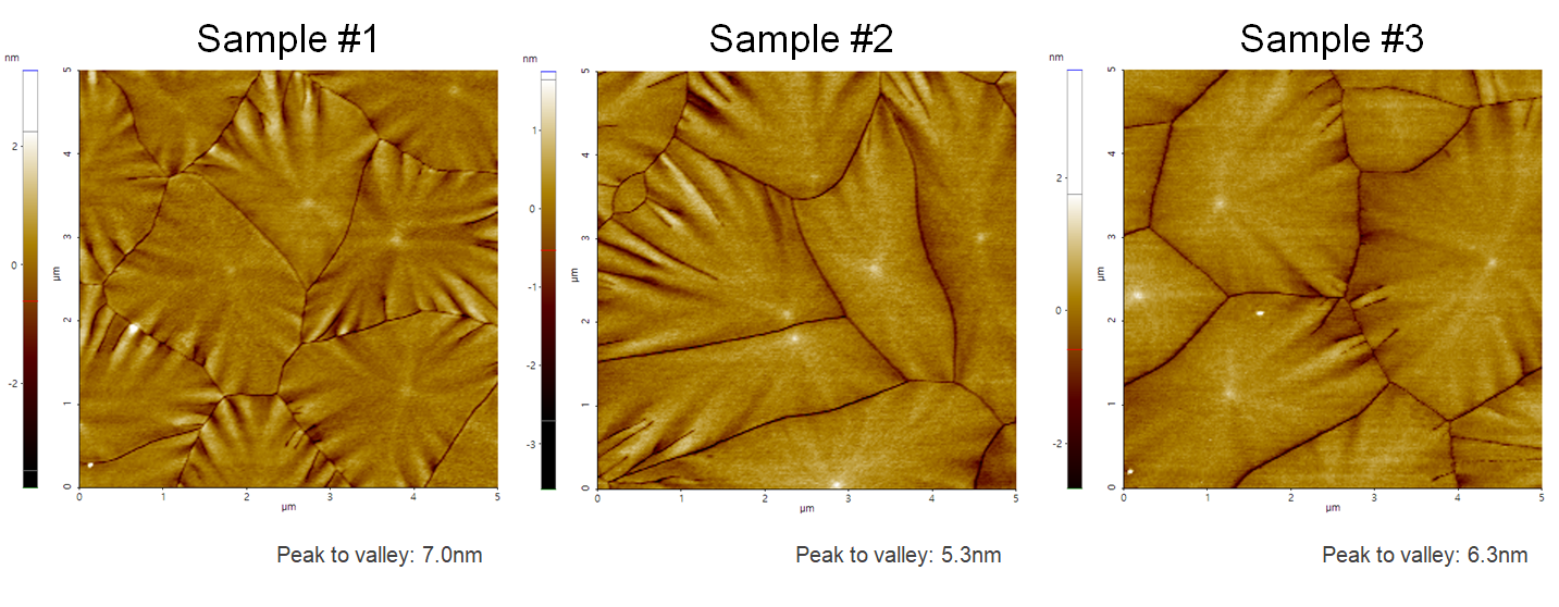
ITO-film, which was sputter deposited onto silicon. The grain size of those samples was influenced by changing the process settings in the Cluterline RAD sputter deposition system, one of the deposition tool platforms manufactured by Evatec.
Scanning Conditions
- System: NX10
- Scan Mode: Non-contact
- Cantilever: PPP-EFM (k=2.8N/m, f=75kHz)
- Scan Size: 5μm×5μm
- Scan Rate: 0.1Hz
- Pixel Size: 256 × 256
- Scan Mode: Non-contact
- Cantilever: PPP-EFM (k=2.8N/m, f=75kHz)
- Scan Size: 5μm×5μm
- Scan Rate: 0.1Hz
- Pixel Size: 256 × 256