-
Lift Yeditepe_University OpticalWaveguides DomainSwitching Trench Treatment HACrystal Magnetic Force Microscopy BismuthVanadate Cell norganic TCS TemperatureControlledAFM Tape Aluminum CNT SoftSample graphene_hybrid FM_KPFM PolyimideFilm Mechanical&nanotechnology ForceVolume self_healing PhaseTransition LeakageCurrent MolecularSelfAssembly TriGlycineSulphate SThM Wonseok Piezoresponse Annealing VinylAlcohol Corrosion DOE Jason
Report image
If you found this image unacceptable, please let us know. We will review your report and take action if we determine this image is really unacceptable.
Tungsten coated wafer
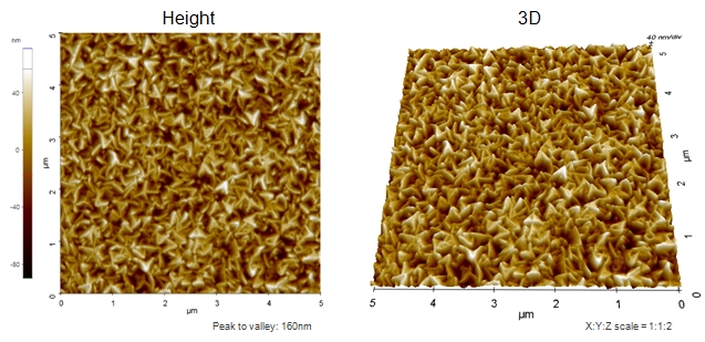
Scanning Conditions
- System: NX10
- Scan Mode: NCM
- Cantilever: NCHR (k=42N/m, f=300kHz)
- Scan Size: 5μm×5μm
- Scan Rate: 0.3Hz
- Pixel: 512×5126