-
DeflectionOptics LightEmiting Oxide InLiquid Fiber HexagonalBoronNitride OpticalModulator PyroelectricDetector Optic SThM Vanadate Temperature Graphite PVAC molecular_self_assembly Electrode KPFM DomainSwitching PinpointPFM Global_Comm fifber Typhimurium ScanningKelvinProbeMicroscopy Friction Piezoresponse SingleLayer DNA Deposition TungstenDeposition thermal_conductivity LaAlO3 FM_KPFM Battery PinpointNanomechanicalMode YttriaStabilizedZirconia
Report image
If you found this image unacceptable, please let us know. We will review your report and take action if we determine this image is really unacceptable.
WLI image of wafer ID mark
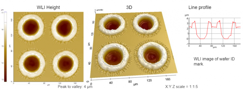
Scanning Conditions
- System : NX-Hybrid WLI
- Scan Mode: WLI
- Field of view: 182μm×182μm