-
ForceVolume Fendb DomainSwitching medical ScanningThermalMicroscopy Ucl Pattern DeflectionOptics hard_disk PS_PVAC Fet PVA HACrystal polymeric_arrays aluminum_nitride food Oxidation Hexylthiophene Perovskite SoftSample Wang Growth Phenanthrene atomic_layer PolymerPatterns MolecularSelfAssembly IRDetector Carbon FM-KPFM Flake Blood ScanningKelvinProbeMicroscopy Polyimide molecular_beam TPU
Report image
If you found this image unacceptable, please let us know. We will review your report and take action if we determine this image is really unacceptable.
Semiconductor device, Failure analysis
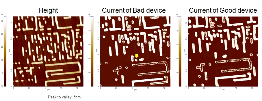
Scanning Conditions
- System: NX10
- Scan Mode: Conductive AFM
- Cantilever: CDT-Contr (k=0.5N/m, f=20kHz)
- Scan Size: 11μm×11μm
- Scan Rate: 1Hz
- Pixel: 512×512
- Sample bias: -0.5V