-
Switching OpticalWaveguide Subhajjit I-VSpectroscopy HanyangUniv Ito AdhesionForce LiquidCrystal Hole bias_mode Scanning_Thermal_Microscopy VortexCore Imprint temperature controller AFM ferromagnetic FloppyDisk AEAPDES ULCA Bacterium Sphere WPlug Barium_titanate SRAM Jason Hydroxyapatite Chemical Vapor Deposition AM_KPFM MultiferroicMaterials GlassTemp Co/Cr/Pt Cross-section semifluorinated_alkanes YszSubstrate Piranha VerticalPFM
Report image
If you found this image unacceptable, please let us know. We will review your report and take action if we determine this image is really unacceptable.
Christmas Ball Lithography on Si
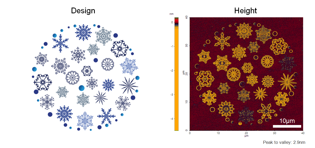
Create oxidation layers on bare Si surface using bias mode of lithography.
Scanning Conditions
- System: NX10
- Scan Mode: Lithography
- Cantilever: AD-40-SS (k=40N/m, f=200kHz)
- Scan Size: 40μm×40μm
- Scan Rate: 0.5Hz
- Pixel Size: 1024 × 1024
- Tip Bias: -10V for patterened area
- Scan Mode: Lithography
- Cantilever: AD-40-SS (k=40N/m, f=200kHz)
- Scan Size: 40μm×40μm
- Scan Rate: 0.5Hz
- Pixel Size: 1024 × 1024
- Tip Bias: -10V for patterened area