-
GaP Treatment HighAspect ScanningIon-ConductanceMicroscopy Graphene contact Phosphide KAIST F14H20 UnivOfMaryland light_emission Vortex Sidewall fluoroalkane Piezo ElectrostaticForceMicroscopy Hair I-VSpectroscopy Corrosion PVA DeoxyribonucleicAcid Potential PolyimideFilm vertical_PFM polymeric_arrays Defects EFM Polyimide WPlug OpticalWaveguide ForceVolume LiNbO3 Etch Pinpoint Carbon
Report image
If you found this image unacceptable, please let us know. We will review your report and take action if we determine this image is really unacceptable.
Trench Etch Profile on Si Wafer
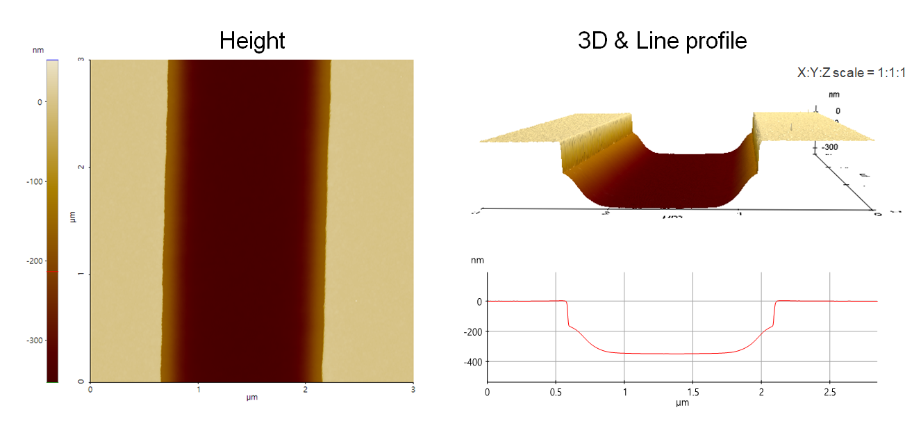
Top dielectric trench etch profile on Si wafer having tapered slope at the trench sidewall.
Scanning Conditions
- System: NX20
- Scan Mode: Non-contact
- Cantilever: AC160TS (k=26N/m, f=300kHz)
- Scan Size: 3μm×3μm
- Scan Rate: 0.21Hz
- Pixel: 1024 × 256
- Scan Mode: Non-contact
- Cantilever: AC160TS (k=26N/m, f=300kHz)
- Scan Size: 3μm×3μm
- Scan Rate: 0.21Hz
- Pixel: 1024 × 256