-
MonoLayer EPFL ThinFilm SingleCrystal molecules Mobile Composition mechanical_property Strontium Heating FM-KPFM FailureAnalysis ferromagnetic CopperFoil Singapore ThermalProperties Galfenol MolybdenumDisulfide Scratch Array LateralForce light_emitting Genetic ThermalConductivity ElectroDeposition Annealing dielectric_trench FastScan thermoplastic_elastomers oxide_layer aluminum_nitride ImideMonomer Optic IRDetector Etch
Report image
If you found this image unacceptable, please let us know. We will review your report and take action if we determine this image is really unacceptable.
Atomic steps on GaP(Gallium Phosphide) layer on Si
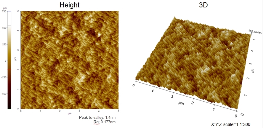
Scanning Conditions
- System: NX20
- Scan Mode: Non-contact
- Cantilever: PPP-NCHR (k=42N/m, f=300kHz)
- Scan Size: 5μm×5μm
- Scan Rate: 1Hz
- Pixel: 512×512