-
Composite ito_film neodymium_magnets GlassTemp PS_PVAC electrospinning BiVO4 CP-AFM graphene_hybrid PinPointMode LightEmiting PMNPT FailureAnalysis FailureAnlaysis Electronics C60H122 Insulator Beads fifber dielectric trench Led Jason Pores PS_LDPE Fluoride Butterfly PetruPoni CuSubstrate Epoxy Indium_tin_oxide Water EvatecAG InsulatorFilm FrictionalForce CopperFoil
Report image
If you found this image unacceptable, please let us know. We will review your report and take action if we determine this image is really unacceptable.
Atomic steps on STO(110)
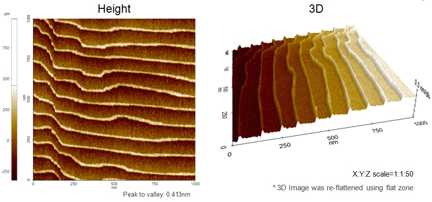
Scanning Conditions
- System: NX10
- Scan Mode: Non-contact
- Cantilever: PPP-NCHR (k=42N/m, f=300kHz)
- Scan Size: 1μm×1μm
- Scan Rate: 0.62Hz
- Pixel: 512×512