-
aluminum_nitride thermal_conductivity ito_film Forevision light_emitting CBD Mechanical Organic Patterns ConductingPolymer Pipette MagneticArray EPFL Boron lithography EvatecAG EFMAmplitude atomic_steps AM-KPFM CuSubstrate AtomicLayer Polyvinylidene_fluoride TemperatureControl LiquidCrystal LifeScience FrictionalForceMicroscopy Pattern Bio Ni-FeAlloy Switching Ito semifluorinated_alkanes neodymium_magnets Stiffness HfO2
Report image
If you found this image unacceptable, please let us know. We will review your report and take action if we determine this image is really unacceptable.
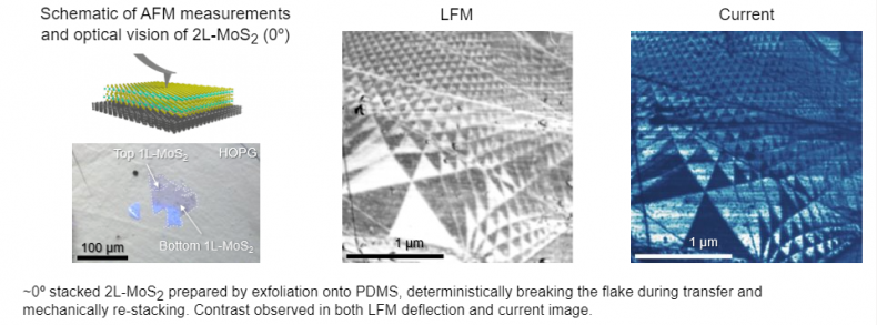
2L-MoS₂ (1/3)

Scanning Conditions
- System : FX40
- Sample bias: 0.25 V
- Scan Mode: C-AFM, LFM
- Scan Rate : 4 Hz
- Scan Size : 2.5μm×2.5μm
- Pixel Size : 512×512
- Cantilever : ContSCPt (k=0.2N/m, f=25kHz)
