-
Magnetostrictive Yeditepe Chrome Writing TemperatureControlledAFM high_resolution suspended_graphene Electronics Foil aluminum_nitride hydrocarbon ScanningThermalMicroscopy PhaseTransition PANI Moire BismuthFerrite Electrical&Electronics PolyimideFilm Step silicon_carbide Neodymium Perovskite AEAPDES Mobile kelvin probe force microscopy Change Conductive AFM ContactModeDots molecular_self_assembly Aluminium_Oxide ThermalDetectors LiIonBattery FAPbI3 LFM FFM
Report image
If you found this image unacceptable, please let us know. We will review your report and take action if we determine this image is really unacceptable.
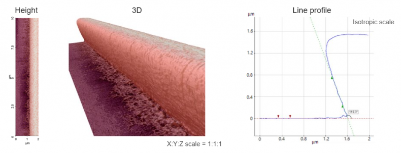
Photoresist pattern (post-development process)

Scanning Conditions
- System : NX-3DM
- Scan Mode: Non-contact
- Scan Rate : 0.1 Hz
- Scan Size : 2μm×10μm
- Pixel Size : 512×2048
- Cantilever : EBD-R2-NCLR (k=45N/m, f=190kHz)
