-
BTO Materials Sadowski Beads BiasMode self-assembly CuSubstrate VerticalPFM Regensburg Polymer Calcium CuParticle ScratchMode PolyvinylideneFluoride MagneticArray NUSNNI Crystal ChemicalCompound ShenYang Resistance fluoroalkane contact Oxide LowDensityPolyethylene CarbonNanotube Flake dielectric trench dielectric_trench dichalcogenide hetero_structure LFM PDMS Modulus KAIST Pore
Report image
If you found this image unacceptable, please let us know. We will review your report and take action if we determine this image is really unacceptable.
Chip
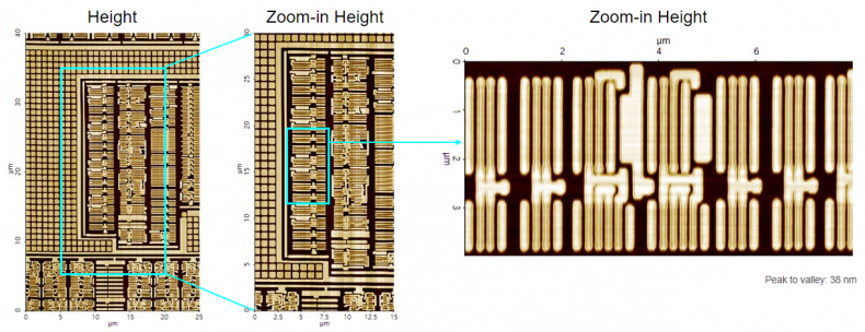
Scanning Conditions
- System : NX-Wafer
- Scan Mode: Non-contact
- Scan Rate : All 1Hz
- Scan Size : 25μm×40μm, 15μm×40μm, 8μm×4μm
- Pixel Size : 2048×256, 2048×256, 1024×256
- Cantilever : OMCL-AC160TS(k=26N/m, f=300kHz)