-
Typhimurium LateralForceMicroscopy Melt Ecoli Scanning_Thermal_Microscopy PyroelectricDetector Gallium_Arsenide RedBloodCell Al2O3 PolyvinylAcetate WPlug FFM plastic Sio2 MolecularSelfAssembly FM_SKPM Tapping Barium_titanate CuParticle Zagreb Blend GalliumPhosphide YttriaStabilizedZirconia Cross-section MechanicalProperty Boundary SmallScan 2dMaterials Fiber Polypropylene Lattice Bio SiliconeOxide MultiLayerCeramicCapacitor VerticalPFM
Report image
If you found this image unacceptable, please let us know. We will review your report and take action if we determine this image is really unacceptable.
PS/LPDE
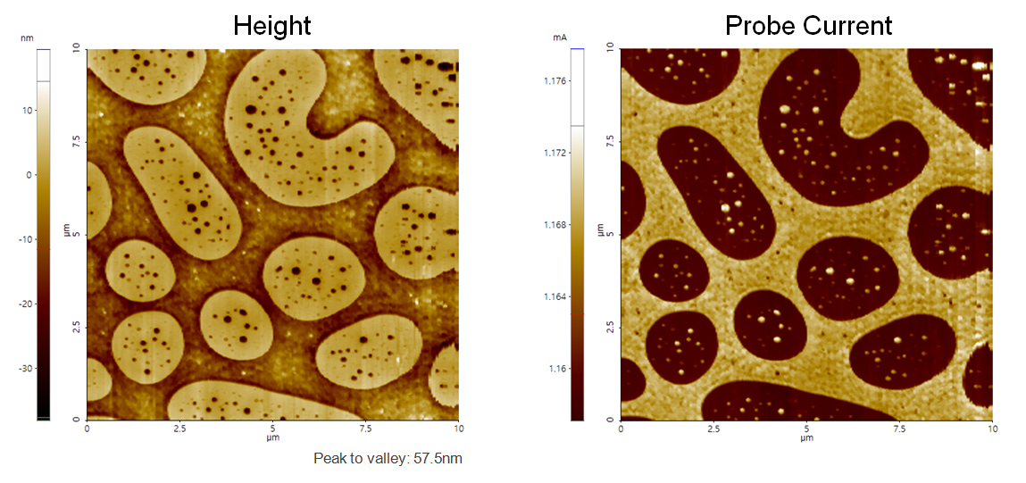
Spincast layer of PS/LDPE blend on Si. Signal change by thermal conductivity difference.
Scanning Conditions
- System: NX10
- Scan Mode: SThM
- Cantilever: NanoThermal Probe
- Scan Size: 10μm×10μm
- Scan Rate: 0.5Hz
- Pixel Size: 256 × 512
- Scan Mode: SThM
- Cantilever: NanoThermal Probe
- Scan Size: 10μm×10μm
- Scan Rate: 0.5Hz
- Pixel Size: 256 × 512