-
Electical&Electronics MagneticForce Graphite Sadowski NCM\ Logo CrystalGrowing Tapping LateralPFM Fluoride bias_mode PetruPoni LiNbO3 semifluorinated_alkane hard_disk Domain Morphology Hole Treatment AM_SKPM EFM Au111 Wonseok Tungsten_disulfide Sidewall Croatia EPFL C36H74 hard_disk_media Led Pvdf Roughness India pulsed_laser_deposition hydrocarbon
Report image
If you found this image unacceptable, please let us know. We will review your report and take action if we determine this image is really unacceptable.
Taegeuk Mark Lithography on PZT
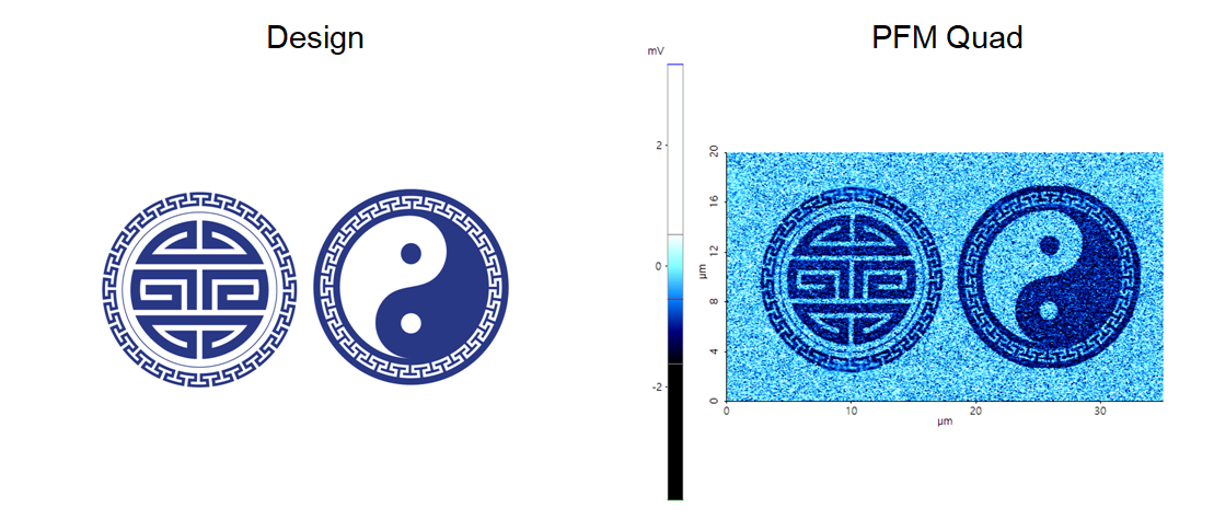
Re-arranged the domain pole direction on PZT surface using bias mode of lithography.
Scanning Conditions
- System: NX10
- Scan Mode: Lithography
- Cantilever: PPP-ContScPt (k=0.2N/m, f=25kHz)
- Scan Size: 35μm×20μm
- Scan Rate: 0.5Hz
- Pixel Size: 1024 × 1024
- Tip Bias: 10V for patterned area
- Scan Mode: Lithography
- Cantilever: PPP-ContScPt (k=0.2N/m, f=25kHz)
- Scan Size: 35μm×20μm
- Scan Rate: 0.5Hz
- Pixel Size: 1024 × 1024
- Tip Bias: 10V for patterned area