-
Hafnium_dioxide OrganicSemiconductor CntFilm LiquidCell BiFeO3 MagneticArray ThinFilm food Piezo self-assembled_monolayer Magnets China Spain Electrical&Electronics PpLdpe BariumTitanate Mechanical&nanotechnology Phthalocyanine Logo Regensburg Copolymer Magnetic Force Microscopy GlassTemperature PolyvinylideneFluoride STO Phosphide ferromagnetic Bismuth DeflectionOptics Nanotechnology Ecoli Spincast epitaxy FrequencyModulation OpticalModulator
Report image
If you found this image unacceptable, please let us know. We will review your report and take action if we determine this image is really unacceptable.
AlN/GaN/AlN Hetero Structure
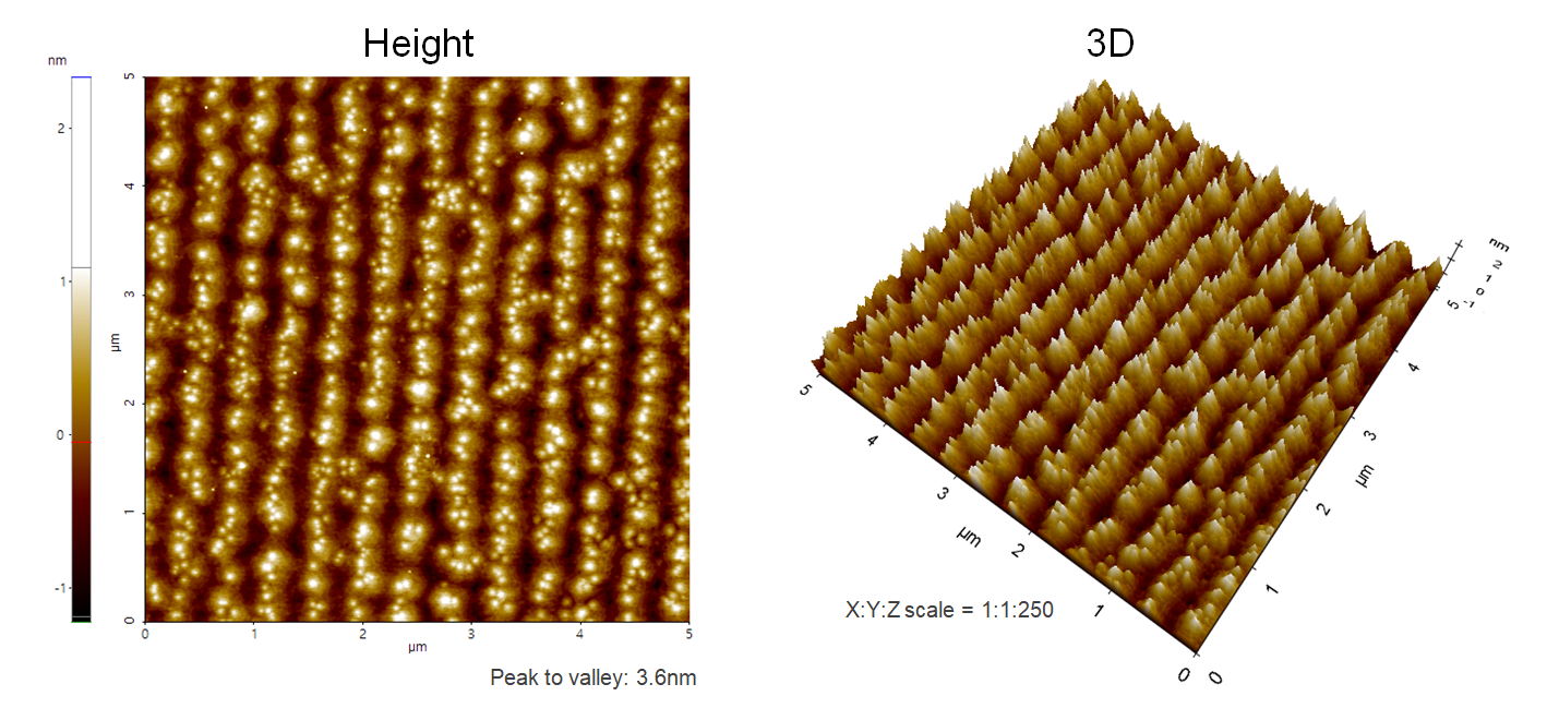
AlN/GaN/AlN hetero structure grown on SiC substrate by Molecular Beam Epitaxy (MBE) system.
Scanning Conditions
- System: NX20
- Scan Mode: Non-contact
- Cantilever: AC160TS (k=26N/m, f=300kHz)
- Scan Size: 5μm×5μm
- Scan Rate: 0.5Hz
- Pixel Size: 512 × 512
- Scan Mode: Non-contact
- Cantilever: AC160TS (k=26N/m, f=300kHz)
- Scan Size: 5μm×5μm
- Scan Rate: 0.5Hz
- Pixel Size: 512 × 512