Thin Films Nanolithography (XEL)
Thin Films Nanolithography (XEL)
Scanning Probe Nanolithography is a very promising technology for nanofabrication. It uses the probe tip of scanning probe microscope to manipulate materials at nanometer scale. There are many ways to to make patterns, such as mechanical scratching and electrical field oxidation. Park System provides a very powerful software, XEL, for Nanolithography. It supports a variety of lithography modes such as Z scanner movement mode, Set point mode, and Bias mode. It supports both Vector and Raster scan modes.

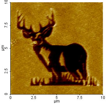
Figure 1. A Big Buck pattern made on a silicon substrate using bias mode XEL Nanolithography. The pattern is made on a silicon surface using the Raster scan mode.
Publications Using XE-AFM and Nanolithography
AA Milner, K Zhang, and Y Prior; Floating Tip Nanolithography; NanoLetters; 2008 Vol. 8, No. 7; 2017-2022
Equipment: Park Systems XE-120

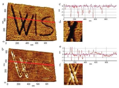
Figure 2. (a) Hot floating tip writing WIS (for the Weizmann Institute of Science) on AZ4620 photoresist film. The writing speed was 50 nm/sec at tip-sample gap 3 ( 2 nm and the average laser power was ∼3 × 10⁵ W/cm2. (b) Direct mechanical scratching of the same polymer with an identical cold tip. Profiles c and e correspond to the red cross-section lines in panels a and b; images d and f are the magnified line intersections in panels a and b, respectively.
Abstract: We demonstrate noncontact, high quality surface modification of soft and hard materials with spatial resolution of ∼20 nm. The nanowriting is based on the interaction between the surface and the tip of a standard atomic force microscope illuminated by a focused femtosecond laser beam and hovering (at ambient conditions) 1-4 nanometers above the surface without touching it. Field enhancement at the tip-sample gap or high tip temperature are identified as the causes of material ablation.
