Characterizing Silanized Surfaces with Imaging Ellipsometry
PHILIPP JÄHDE, PETER H. THIESEN
Material:
Imaging ellipsometry is applied to characterize homogeneous and patterned silane coats on different substrates.
This compendium addresses the following topics:
• Imaging of silane mono- and multilayers on silicon wafers
• Soft Lithography deposition of silane patterns on silicon, steel and glass
• Detection of pattern irregularities and printing artifacts
• Modelling of silane layer thickness from spectroscopic ellipsometry data
Introduction
Silanes are monomeric silicon compounds, which were first described in the middle of the 19. century. They are structurally analogous to the carbon-based alkanes and exhibit similar physical properties. Since silicon is more electropositive than carbon, their chemical properties though can differ a lot from alkanes [1,2].
One of the most important reactions silanes can undergo is the formation of very strong –Si-O bonds with hydroxyl groups on the surface of glass, metals or minerals. Depending on the remaining functional groups of the bound silanes, this modification can lead to tremendous changes in the surface properties of the substrate.[3,4]
Silanes bearing organophilic functional groups can facilitate bonds of organic substances to inorganic substrates and are therefore important coupling agents and adhesion promoters for a wide variety of industrial and medical processes. Another important application is the use as very durable hydrophobing coats for otherwise hydrophilic inorganic surfaces [5,6,7].
To achieve these surface modifications, the silane ideally has to form a monolayer on the inorganic substrate. To analyze these nanometer-thin films, Imaging Ellipsometry offers a contact-free, nondestructive measuring method capable of resolving thickness differences between silane mono- and bilayers. The micrometer scale xy-resolution offers the possibility to characterize patterned silanization as well as to detect variations in homogeneous films.
Imaging Ellipsometry ± what makes the difference?

Figure 1. EP4 with illumination arm on the left and Analyzer arm at the right. The sample can be placed onto a motorized xy-table.
Imaging Ellipsometry (IE) has the benefit of combining the measurement quantities of ellipsometry with the lateral resolution of microscopy. A user will get ellipsometric enhanced contrast micrographs, thickness and optical constants distribution of its sample, that is measured by the ellipsometric plattform EP4 (Figure 1).
In general, the thickness measurements with an ellipsometer are nondestructive and highly accurate. In the most cases, the optical constants can be determined independently.
To measure micro sized structures conventional ellipsometry uses a focused light spot. The lateral ellipsometric resolution is thereby limited by the spot size that may go down to approx. 50 µm.
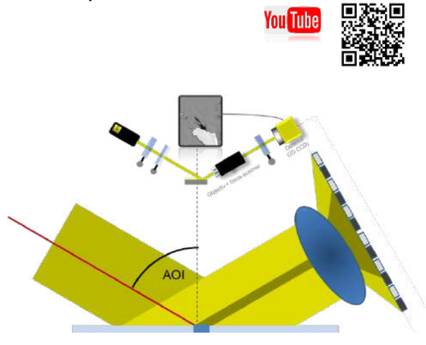
Figure 2. EP4 with illumination arm on the left and Analyzer arm with the optical system at the right. The sample can be placed onto a motorized xy-table.
In IE the sample is illuminated with collimated light as shown in Figure 2. The lateral ellipsometric resolution is only limited by the objective and the CCDcamera used as detector. With this method a lateral ellipsometric resolution down to 1 µm can be reached.
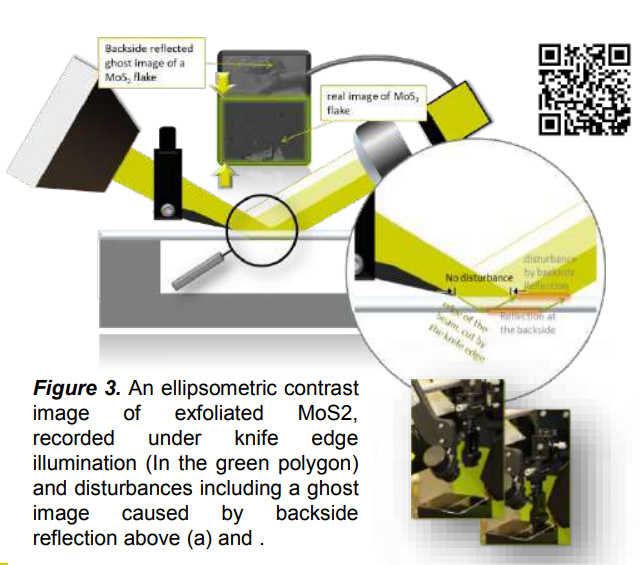
The CCD-camera offers a live view of the sample. By the rotation of the polarizing components, Delta ǻ and Psi Ȍ can be measured for every pixel. The user will see the progress and the change in contrast by different polarizations in the live view. The user can also select the area to measure on the contrast image seen in the live view. In contrast to conventional ellipsometry, where the measured region is chosen by the position of the spot, the user in IE can select the measured region in the contrast view at the detector side. This selection enables the use of knife edge illumination – a unique tool to measure thin films on transparent substrates. Figure 3 shows a micrograph of MoS2 on sapphire. The ghost image on the upper part occurs from the disturbing backside reflections. By the combination of detector side selection and knife edge illumination the user can perform valid ellipsometric measurements inside the green polygon.
Thickness measurement of homogeneous silane layers
To use silanes as coupling agents between different substances, homogeneous monolayers have to be applied to the substrate, since a linkage via multiple polymerized silane molecules is much weaker than the direct coupling via a single molecule. To assess the thickness and homogeneity of such layers, measuring methods are necessary which can resolve layer thickness at single-molecule resolution as well as provide sufficient x/yresolution to characterize local thickness variations. Commonly used methods are Atomic Force Microscopy (AFM), water contact angle measurement, low-angle xray reflectivity and Ellipsometry [8,9]. Besides providing the necessary spatial resolution, Imaging Ellipsometry also offers high imaging speed, contact-free, nondestructive measurement and the calculation of optical parameters of the applied layers.
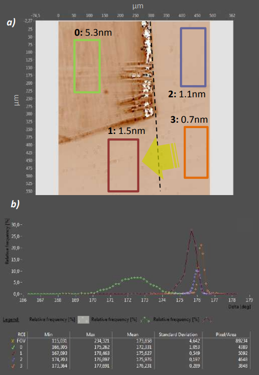
Figure 4. a) Delta map of homogeneous silane films. 0) multilayer of GLYMO, 5.3nm thickness 1) remaining GLYMO layer after toluene cleaning, 1.5nm thickness 2) Vapor phase deposition of GLYMO 3) residual vapor phase deposition of GLYMO after toluene wiping Transparent arrow indicates wiping direction b) Histograms of ROIS 0-3. The more homogeneous ROIs 1-3 result in narrower distributions with much lower STD than the less homogeneous ROI 0.
In Fig. 4 a), an ellipsometric ǻ-map of a Si/SiO2-substrate with an applied layer of (3-Glycidyloxypropyl)trimethoxysilane (GLYMO) is shown (the silane was applied on the whole left side of the dashed line). The Imaging Ellipsometer reveals thickness differences between regions with different post-silane application treatment: ROI 0 is the untreated silane coat with a thickness of 5.3nm. In ROI 1, the lower half of the silane layer has been wiped from right to left with toluene to remove unbound GLYMO, which led to a thickness reduction of 3.8nm. Region 2 and 3 were not in direct contact with the silane during application, the 1.1nm layer in ROI 2 is most likely created via vapor phase deposition of evaporating silane during the application process. The further reduction of the layer thickness in ROI 3 after toluene wiping shows that also in the vapor phase deposited layer unbound silane is present. The residual 0.7nm layer thickness is in the range of one GLYMO molecule length, though it rather represents a thickness average in a one-pixel sized surface area: Since the silanol group coverage on the wafer surface is not 100%, regions with bound silane and blank wafer areas average within the µm-range pixel to the detected 0.7nm.
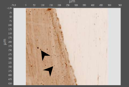
Figure 5. Ellipsometric Delta maps of APDMES on Si/SiO2: Polymerized APDMES spots in the silane coat (left area) are clearly resolved by Imaging Ellipsometry (arrows indicate just two example spots)
One problem during the application of silane layers is the polymerization between silane molecules themselves, which leads to inhomogeneous surfaces with weaklybound spots of polymerized silane. The amount of polymerization depends amongst others on the used solvent, silane concentration, humidity and temperature and can be easily measured with Imaging Ellipsometry. Fig. 5 shows a layer of 3- Aminopropyl(diethoxy)methylsilane (APDMES) on Si/SiO2, where polymerized silane spots are detected in the Imaging Ellipsometry data.
Patterned silanization via microcontact printing
While homogeneous silane coats are usually applied via vapor phase deposition, dip coating or simple painting, patterned silane layers are created with comparatively simple microcontact printing or photolithography-based methods capable of assembling complex 3Dpatterns of multiple silanes [10,11].
Patterned silanization is used in many biological high-throughput applications such as lab on a chip-systems, NextGenSequencing and microarray fabrication to tether proteins, DNA and reagents to various substrates. In microelectronics it offers the possibility to integrate organic structures with inorganic semiconductor subtrates.
All of these applications require a precise replication of the desired silane layer pattern and thus a method to measure parameters like thickness, edge sharpness and structure size. The micrometer-x/yresolution of Imaging Ellipsometry and its high imaging speed make it a valuable tool to assess these parameters not only in research, but also in quality control of large-scale patterning processes.
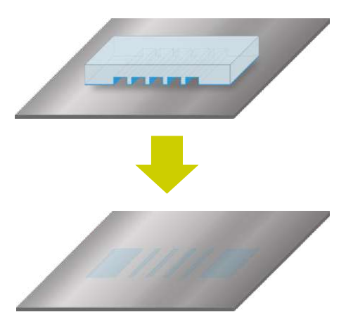
Figure 6. Microcontact printing procedure: Silane solutions were applied to a microstructured stamp made of Polydimethylsiloxane (PDMS, Sylgard 182). After drying of the silane solution, the stamp was pressed onto RCA-1 cleaned silicon wafers, polished steel and glass for 30 minutes. The stamp pattern was a grating with 20µm wide printing bars and 50µm wide non-printing gaps.
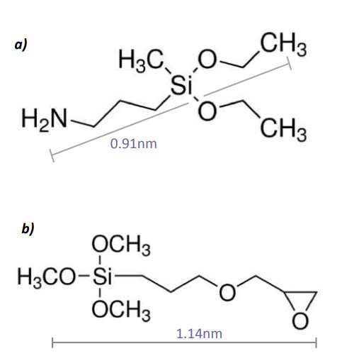
Figure 7. a) Structural formula of 3-Aminopropyl(diethoxy) methylsilane b) Structural formula of (3-Glycidyloxypropyl)trimethoxysilane Both silanes were diluted in Toluene (5mmol/l)
Characterization of patterned silane layers
The contact printing procedure described in Figure 6 is sufficient to transfer a silane layer closely replicating the stamp pattern to silicon wafers. Figure 8a shows a Delta map of stamped APDMES on Si/SiO2 detected with Imaging Ellipsometry. The 20µm/50µm grating seems to be precisely reproduced, though the spatial resolution of Imaging Ellipsometry reveals a problem of the applied printing approach: If only histograms of a printing (ROI1) and a nonprinting region (ROI0) are compared, a clear Delta-shift is observed, resulting in two distinct pixel value distributions with a difference of 0.24° between their means (Fig. 8b). Again, this corresponds to pixel sized averages.
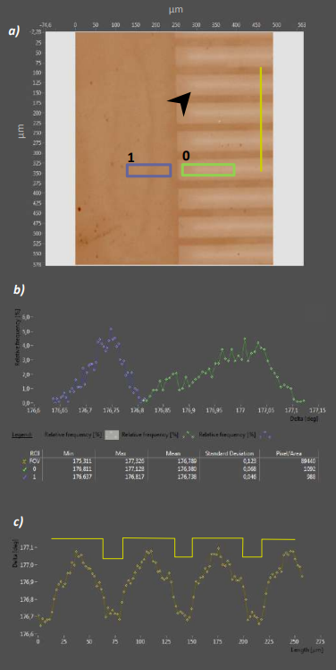
Figure 8. a) Delta map of a patterned APDMES film. The 20µm/50µm grating is clearly reproduced in the µC-printed layer. Arrowhead indicates silane gradients within non-printing gaps. b) Delta Histogram of ROIs 0 and 1. APDMES application leads to a 0.25° Delta difference compared to the non-printed ROI 0 c) Line profile across the printed grating. The plot reveals soft borders between contact printed- and non-printed regions.
Analyzing the pattern fidelity with a line profile (Fig. 8c) instead obviously shows, that the distinct edges of the grating are not replicated in the printed pattern. Instead, a Delta gradient from the edges to the center of the non-printing gaps is measured (Arrow in Fig. 8a). This gradient results from silane solution menisci forming at the lower edges of the stamp gaps [12]. If these menisci are still present during the printing procedure, their evaporation leads to vapor phase deposition of silane in non-printing regions. To prevent this effect, the stamp has to be completely dry before it is applied to the substrate. Longer drying time though also leads to stronger polymerization of the silane on the stamp (especially at high air humidity), degrading the quality of the printed silane layer.
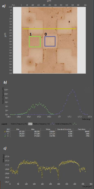
Figure 9. a) Delta map of a patterned APDMES film. The X in the stamp label is clearly reproduced in the µC-printed layer. b) Delta Histogram of ROIs 0 and 1. APDMES application leads to a 0.33° Delta difference compared to the non-printed ROI 0 c) Line profile across the printed letter. Borders are sharper than in Fig.8 and the non-printed surface is flatter.
In Figure 9, a APDMES print from a stamp with longer drying time (10 vs. 5 minutes) is shown. The printed edges are more defined now, and show a steeper step between printing- (ROI 1) and non-printing regions (ROI 0). The Delta distribution of the nonprinting region is also slightly right-shifted compared to Figure 8 (mean 177.123° vs. 176.98°) and has a lower STD, indicating an on pixel average thinner residual silane layer lacking the gradient seen before.
As a drawback, small dots of polymerized APDMES are now visible across the printed surface. A possible solution to these problems is the „stamp pad“ approach described by Pompe et al. [12], where the silane solution is not directly applied to the stamp, but rather picked up from a PDMS surface wetted with silane solution to prevent excess capillary condensation in the stamp gaps.
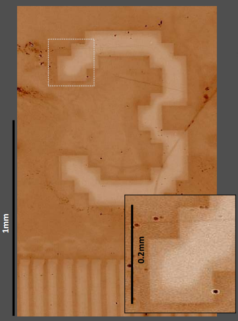
Figure 10: High-resolution stitched Delta map of a patterned APDMES film automatically generated from 25 individual maps
These measurements can also be performed on large patterned samples. The sample is then automatically moved on a motorized stage and the resulting individual maps are fused to one large map. Figure 10 shows a larger region of the printed wafer consisting of 25 individual maps. Macro- and microscopic surface irregularities can thus be analyzed in the same map.
Modeling of silane layer thickness
Ellipsometry is a model-based method. This means that one does not get a direct value of the wanted physical quantity, e.g. thickness or a refractive index. Instead, one measures the ellipsometric angles ǻ and Ȍ or the samples’ Mueller Matrix, which quantify the sample-induced changes to (polarized) light for isotropic and anisotropic samples respectively. These experimental data then have to be compared to simulated data from an optical model of the sample. In practice, a non-linear fitting algorithm is applied to match the free parameters of the model to the experimental data. If the model is in good agreement with the measured data, it can be deemed appropriate and used to derive physical values from the ellipsometric angles.
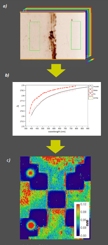
Figure 11: Calculation of thickness maps a) To devise a dispersion model for the applied silane, a spectroscopic set of Delta maps is recorded from a region containing silane coat and blank wafer b) EP4Model is used to fit a Cauchy model to the measured spectral data c) The model can then be used to calculate thickness maps from single wavelength Delta maps of patterned sample regions (calibration bar in nm)
To derive an optical model for an uncharacterized sample like the silane coats shown here, ellipsometric maps are recorded at different illumination wavelengths (Fig.11a). Average Delta values from a silane coated region and a blank Si/SiO2 region are then imported as spectra into the modeling software and used as data for dispersion model fits (Fig. 11b). In the case of SiO2 , APDMES and GLYMO, Cauchy dispersion models were used for fitting.
The optical parameters gained during the fit can afterwards be used to calculate thickness maps from single-wavelength ellipsometric maps of different sample regions or entirely different samples. In Figure 11c, a thickness map of the APDMES layer on Si/SiO2 has been calculated from the Delta/Psi map shown in Figure 9a.
Microcontact printing of silane layers on steel
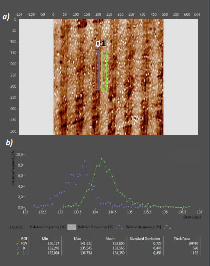
Figure 12: Patterned silanization of steel a) Delta map of a patterned APDMES film on polished steel. The µCprinted 20µm/50µm grating is detectable with Imaging Ellipsometry despite the uneven steel substrate b) Delta Histogram of ROIs 0 and 1. APDMES application leads to a 0.7° Delta difference compared to the non-printed ROI 0
As an optical, non-destructive method, IE is almost independent from the substrate onto which a silane layer is applied. Microcontact printing on polished steel with the same approach as used for hydrophilized silicon wafers leads to distinguishable silane patterns (Fig. 12a). Delta distributions in both printed and unprinted regions show a larger STDev compared to prints on Si wafers, reflecting the more inhomogeneous surface of the polished steel (Fig. 12b). The capability of Imaging Ellipsometry to resolve the silane layer even on this imperfect surface shows its potential for the application outside of clean room- or laboratory environments
Microcontact printing of silane layers on rough glass
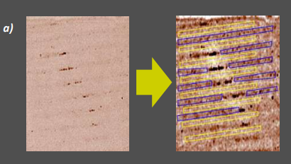
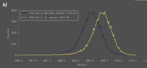
Figure 13: Patterned silanization of glass a) Delta map of a patterned APDMES film on glass (black spots are polymerized silane and were excluded from histogram calculation). Noise filtering in ImageJ makes printed- and unprinted regions sufficiently distinguishable for multi ROI-selection b) Resulting Delta map histogram of ROIs shown in 13a
Printing the APDMES grating on rough glass (an etched microscope slide) yields a silane layer almost indistinguishable from the glass surface even under beamcutter illumination and optimized angle of view (Fig. 13a).
To perform further data processing on difficult maps as these, DataStudio offers raw data export. In this example, the map was imported to Fiji [13], noise filtered with a bandpass-FFT filter and average histograms were calculated from multiselection ROIs (Fig. 13b). This reveals a 0.34° Delta shift between coated and uncoated ROIs in low SNR-data from a highly scattering substrate.
Protein adsorption on patterned silane layers
A common application for patterned silanization is the tethering of proteins to inorganic substances for bioanalytical processes. Imaging Ellipsometry is not only capable of measuring the thickness of the adsorbed protein layers with high spatial resolution, but can also monitor the temporal kinetics of the adsorption process. By recording time series of Delta- and Psi maps, 4D-information about x/y-location, thickness and change in time can be extracted from the ellipsometric data.
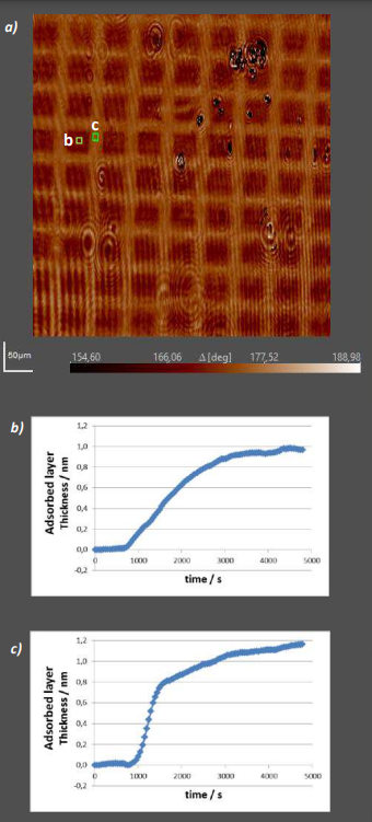
Figure 14: Temporal kinetics of BSA adsorption on OTS patterns a) Si/SiO2 substrate patterned with OTS b) Time course of BSA layer thickness change in an OTS-covered region c) Time course of BSA layer thickness change in a blank wafer region
In the experiment shown in Figure 14, Octadecyltrichlorosilane (OTS) was printed onto a silicon wafer. The wafer was then put in a flow cell continuously perfused with Bovine Serum Albumin (BSA)-solution and Delta/Psi-maps were recorded for 80 minutes.
Figure 14b and c show the time course of the average calculated layer thickness change in ROIs b (OTS) and c (blank Si/SiO2 ). The curves highlight an important advantage of Imaging Ellipsometry’s capability to record time series: While the average maximum layer thickness in both region is quite similar (1.2nm vs. 1nm), the apparent difference between OTSmodified- and blank wafer lies in the maximum slope of the signal. The steeper adsorption curve of the blank region and the slight signal undershoot at 900s might have been overlooked by a measuring method with slower sample rate than imaging Ellipsometry.
Conclusion
Spectroscopic Imaging Ellipsometry is a very powerful tool to characterize, analyze and investigate thicknesses, optical properties and defects or impurities of microstructured and homogeneous silane coats.
It utilizes the polarization properties of samples to extract their dielectric function, from which a multitude of sample properties can be derived. As a purely optical method, it can thus determine the thickness of silane films contact-free and non-destructive, making it applicable not only to R&D, but also to quality control of end products.
Its sub-nanometer layer thickness sensitivity allows the detection of slightest variations in homogeneous silane coats with microscopic x/y-resolution. In patterned silanization applications this spatial resolution obviously offers a tool to assess pattern fidelity and thickness. Due to its working principle based on Delta/Psishifts and the resulting ability to tell apart substances with different optical properties, these patterns are though not restricted to embossed layers of single substances. Instead, also more sophisticated, mosaiclike coats of multiple substances which are only distinct in their x/y-distribution, but of the same layer thickness can be analyzed with Imaging Ellipsometry. The substrate independence of Imaging Ellipsometry and its ability to characterize coatings even on imperfect surfaces makes these benefits available to a very broad range of silanization applications.
Additionally, the possibility to perform Imaging Ellipsometry measurements as time series expands the application of the method to the characterization of dynamic processes, reaching beyond the fabrication into the actual use of silanized surfaces. For any further question or new application ideas, please don’t hesitate to contact the ACCURION Team.
References
[1] F. WÖHLER AND H. BUFF (1857) Ueber eine Verbindung von Silicium mit Wasserstoff. Justus Liebigs Ann. Chem. 103, 218-229.
[2] B. ARKLES (1997) Silanes. Encyclopedia of Chemical Technology, Fourth Edition, 22, 38-69.
[3] B. ARKLES (1997) Silanes. CHEMTECH 7(12), 766-778.
[4] S. ONCLIN, B. J. RAVOO, D. N. RHEINHOUDT (2005) Engineering Silicon Oxide Surfaces Using SelfǦAssembled Monolayers. Angewandte Chemie 44(39), 6282- 6304.
[5] E.P. PLUEDDEMANN (1983) Silane adhesion promoters in coatings. Progress in Organic Coatings 11(3), 297-308.
[6] E. P. PLUEDDEMANN (2012) Reminiscing on silane coupling agents. Journal of Adhesion Science and Technology 5(4), 261-277.
[7] J.P. MATINLINNA, L.V.J. LASSILA, M. OZCAN, A. YLI-URPO AND P.K. VALLITTU (2004) An Introduction to Silanes and Their Clinical Applications in Dentistry, Intl. Journal of Prosthodontics 17(2), 155-164.
[8] S.R. WASSERMAN, G.M. WHITESIDES, I.M. TIDSWELL, B.M. OCKO, P.S. PERSHAN, J.D. AXE (1989) The structure of self-assembled monolayers of alkylsiloxanes on silicon: a comparison of results from ellipsometry and low-angle x-ray reflectivity. J. Am. Chem. Soc. 111(15), 5852-5861.
[9] M. TERRACCIANO, I. REA, J. POLITI, L. DE STEFANO (2013) Optical Characterization of Aminosilane-modified Silicon Dioxide Surface for Biosensing. Journal Of The European Optical Society – Rapid Publications 8.
[10] S. GILLES (2007) Chemical Modification of Silicon Surfaces for the Application in Soft Lithography. Berichte des Forschungszentrums Jülich 4249.
[11] B. KANNAN, R.P. KULKARNI, S. SATYANARAYANA, K. CASTELINO, A. MAJUMDAR (2005) Chemical patterning for the highly specific and programmed assembly of nanostructures, J. Vac. Sci. Technol. B 23(4), 1364-1370.
[12] T. POMPE, A. FERY, S.HERMINGHAUS (1999) Submicron Contact Printing on Silicon Using Stamp Pads. Langmuir 15, 2398-2401.
[13] J. SCHINDELIN, I. ARGANDA-CARRERAS, E. FRISE ET AL. (2012), Fiji: an opensource platform for biological-image analysis, Nature methods 9(7), 676-682
