-
MonoLayer India HighAcpectRatio FuelCell BTO DNAProtein Ceramic mechanical property epitaxy Chemical Vapor Deposition Sapphire plastic ItoGlass PetruPoni_Institute Singapore Polyaniline I-VSpectroscopy FM_KPFM IRDetector BariumTitanate Photovoltaics ULCA SoftSample Vinylpyridine SiliconeOxide polymeric_arrays CompactDisk single_layer DIWafer Topography high_resolution Gallium organic_polymer Biofilm Force-distance
Report image
If you found this image unacceptable, please let us know. We will review your report and take action if we determine this image is really unacceptable.
Chip
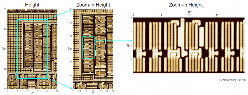
Scanning Conditions
- System : NX-Wafer
- Scan Mode: Non-contact
- Scan Rate : All 1Hz
- Scan Size : 25μm×40μm, 15μm×40μm, 8μm×4μm
- Pixel Size : 2048×256, 2048×256, 1024×256
- Cantilever : OMCL-AC160TS(k=26N/m, f=300kHz)