-
Nanofiber Calcium Conductivity OxideLayer Magnetic MeltingPoint CrossSection Morphology StrontiuTitanate PolymerBlend Graphene Co/Cr/Pt MLCC vertical_PFM SetpointMode Polypropylene DNAProtein GaAs Defect Alkane Piranha Sapphire AnodizedAluminumOxide Wonseok Ecoli Solution SiliconCrystal MonoLayer Oxide GranadaUniv DentalProsthesis Electical&Electronics bias_mode Silicon Tin disulfide
Report image
If you found this image unacceptable, please let us know. We will review your report and take action if we determine this image is really unacceptable.
Stitched image of chiplet
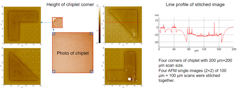
Scanning Conditions
- System : NX-Wafer
- Scan Mode: Non-contact
- Scan Rate : 0.5 Hz
- Scan Size : 100μm×100μm for single image (200μm×200μm stitched image)
- Pixel Size : 512×128 for single image
- Cantilever : OMCL-AC240TS (k=2N/m, f=70kHz)