-
Yeditepe_University CHRYSALIS_INC cannabis Copper I-VSpectroscopy Film OpticalWaveguides HBN HardDiskMedia Silver PhaseChange polyvinyl acetate MfmAmplitude Chungnam_National_University #Materials Biofilm Semiconductor AdhesionEnergy Mfm BlockCopolymer Boundary Conducting Materials NanoLithography Pore Optic Magnetic IcelandSpar University_of_Regensburg thermoplastic_elastomers atomic_layer LiNbO3 HumanHair epitaxy fifber
Report image
If you found this image unacceptable, please let us know. We will review your report and take action if we determine this image is really unacceptable.
Taegeuk Mark Lithography on PZT
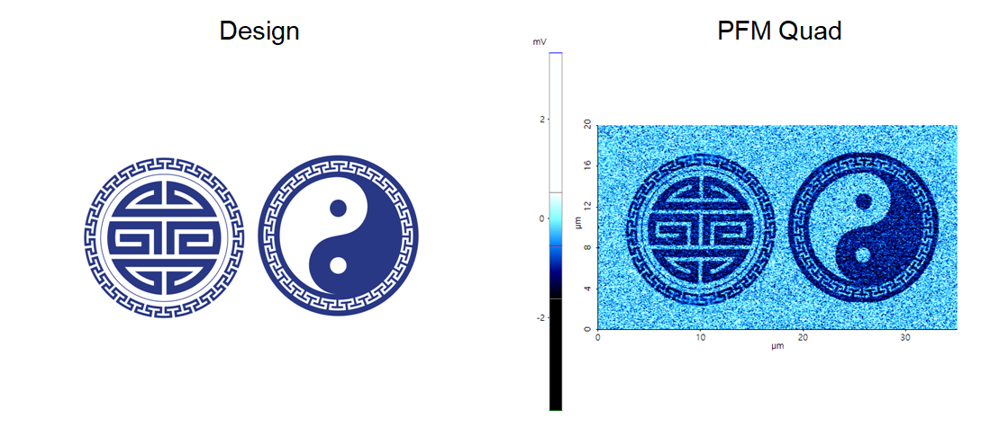
Re-arranged the domain pole direction on PZT surface using bias mode of lithography.
Scanning Conditions
- System: NX10
- Scan Mode: Lithography
- Cantilever: PPP-ContScPt (k=0.2N/m, f=25kHz)
- Scan Size: 35μm×20μm
- Scan Rate: 0.5Hz
- Pixel Size: 1024 × 1024
- Tip Bias: 10V for patterned area
- Scan Mode: Lithography
- Cantilever: PPP-ContScPt (k=0.2N/m, f=25kHz)
- Scan Size: 35μm×20μm
- Scan Rate: 0.5Hz
- Pixel Size: 1024 × 1024
- Tip Bias: 10V for patterned area