-
hard_disk_media Bio PvdfBead Phosphide SoftSample SICM Filter BCZT PECurve DeoxyribonucleicAcid Adhesive KAIST Modulus Chungnam_National_University SolarCell Polymer VortexCore Platinum high_resolution light_emission exfoliate plastic Calcite KPFM Co/Cr/Pt Terrace Bmp Growing atomic_layer dichalcogenide Indium_tin_oxide HOPG CP-AFM oxide_layer Magnetic
Report image
If you found this image unacceptable, please let us know. We will review your report and take action if we determine this image is really unacceptable.
Trench Etch Profile on Si Wafer
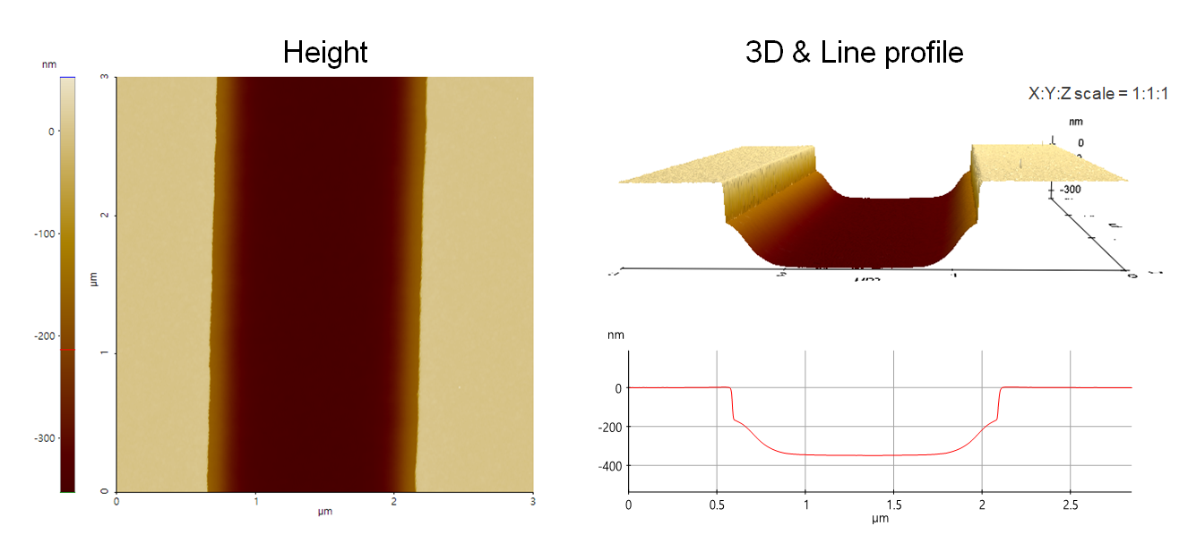
Top dielectric trench etch profile on Si wafer having tapered slope at the trench sidewall.
Scanning Conditions
- System: NX20
- Scan Mode: Non-contact
- Cantilever: AC160TS (k=26N/m, f=300kHz)
- Scan Size: 3μm×3μm
- Scan Rate: 0.21Hz
- Pixel: 1024 × 256
- Scan Mode: Non-contact
- Cantilever: AC160TS (k=26N/m, f=300kHz)
- Scan Size: 3μm×3μm
- Scan Rate: 0.21Hz
- Pixel: 1024 × 256