-
PVA University_of_Regensburg NUS_NNI_Nanocore PtfeFilter margarine CBD MagneticArray multi_layer hard_disk_media Force-distance Topography tip_bias_mode Materials TransitionMetal Boron Pzt Sapphire LiquidCell Phenanthrene Conductive AFM FastScan ScanningTunnelingMicroscopy Corrosion LDPE STM Polytetrafluoroethylene Fujian LFM semifluorinated_alkane SurfaceOxidation PolyvinylideneFluoride YttriaStabilizedZirconia Metal polyvinyl acetate SingleLayer
Report image
If you found this image unacceptable, please let us know. We will review your report and take action if we determine this image is really unacceptable.
GaN epi wafer
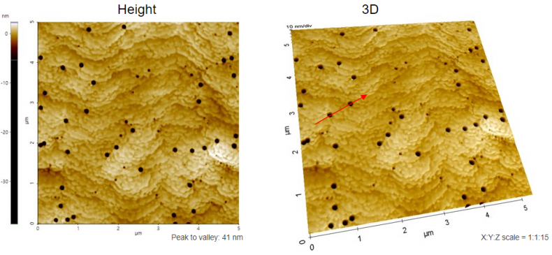
Scanning Conditions
- System : NX-Wafer
- Scan Mode: Non-contact
- Scan Rate : 0.7 Hz
- Scan Size : 5μm×5μm
- Pixel Size : 512×512
- Cantilever : PPP-NCHR (k=42N/m, f=330kHz)