-
Neodymium Photovoltaics Inorganic_Compound #EC LaAlO3 Protein PolyStylene sputter Mobile Platinum Filter exfoliate Melt SrO Ni81Fe19 ItoGlass DeoxyribonucleicAcid ForceVolumeMapping CalciumHydroxide Cross-section Vac TappingMode Potential Force-distance Lateral pulsed_laser_deposition Laser Adhesive PANI Electical&Electronics Morphology NUS_Physics SicMosfet Granada Sphere
Report image
If you found this image unacceptable, please let us know. We will review your report and take action if we determine this image is really unacceptable.
MoS2 Layers on SiO2
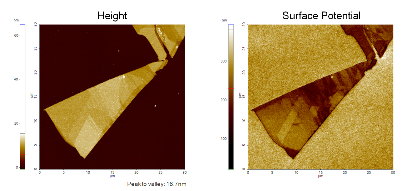
A few layers of MoS2 on SiO2
Scanning Conditions
- System: NX10
- Scan Mode: AM-KPFM
- Cantilever: NSC36Cr-Au B (k=2N/m, f=130kHz)
- Scan Size: 30μm×30μm
- Scan Rate: 0.3Hz
- Pixel Size: 512 × 256
- Scan Mode: AM-KPFM
- Cantilever: NSC36Cr-Au B (k=2N/m, f=130kHz)
- Scan Size: 30μm×30μm
- Scan Rate: 0.3Hz
- Pixel Size: 512 × 256