-
AdhesionForce hard_disk plastics LDPE GalliumPhosphide CarbonNanotube FuelCell Led HumanHair F14H20 Battery Protein Cell INSP Magnetic Force Microscopy self_assembly Monisha Anneal SKPM Sphere PetruPoni_Institute BreastCancerCell KevlarFiber Film DOE Heating SPMLabs Piezoelectric HexacontaneFilm SoftSample Iron PrCurve Oxide Nickel Tin sulfide
Report image
If you found this image unacceptable, please let us know. We will review your report and take action if we determine this image is really unacceptable.
Trench Etch Profile on Si Wafer
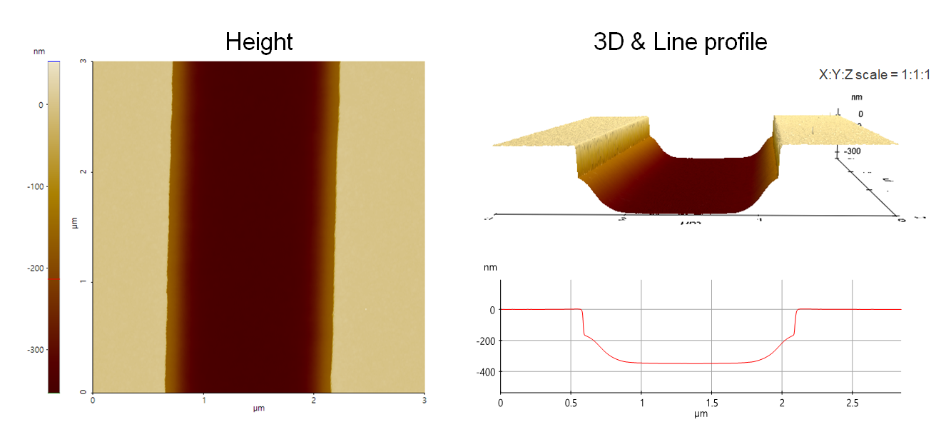
Top dielectric trench etch profile on Si wafer having tapered slope at the trench sidewall.
Scanning Conditions
- System: NX20
- Scan Mode: Non-contact
- Cantilever: AC160TS (k=26N/m, f=300kHz)
- Scan Size: 3μm×3μm
- Scan Rate: 0.21Hz
- Pixel: 1024 × 256
- Scan Mode: Non-contact
- Cantilever: AC160TS (k=26N/m, f=300kHz)
- Scan Size: 3μm×3μm
- Scan Rate: 0.21Hz
- Pixel: 1024 × 256