-
Beads thermal_conductivity PVA Ceramics Morphology Terrace Aggregated_molecules Optoelectronic DeflectionOptics PolycrystallineFerroelectricBCZT Sulfur MolybdenumDisulfide Forevision FrictionForce SAM Zhi EvatecAG Flake Chemical_Vapor_Deposition STO Zagreb Spincast Lateral_Force_Microscopy exfoliate IMT_Bucharest nanobar Permalloy Cobalt PVAP3HT SiWafer Ni-FeAlloy Nanotechnology Film FrequencyModulation Phenanthrene
Report image
If you found this image unacceptable, please let us know. We will review your report and take action if we determine this image is really unacceptable.
ITO Film Sputter Deposited onto Silicon
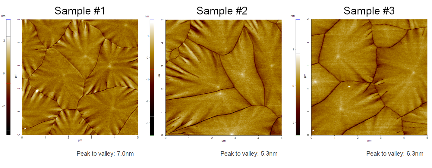
ITO-film, which was sputter deposited onto silicon. The grain size of those samples was influenced by changing the process settings in the Cluterline RAD sputter deposition system, one of the deposition tool platforms manufactured by Evatec.
Scanning Conditions
- System: NX10
- Scan Mode: Non-contact
- Cantilever: PPP-EFM (k=2.8N/m, f=75kHz)
- Scan Size: 5μm×5μm
- Scan Rate: 0.1Hz
- Pixel Size: 256 × 256
- Scan Mode: Non-contact
- Cantilever: PPP-EFM (k=2.8N/m, f=75kHz)
- Scan Size: 5μm×5μm
- Scan Rate: 0.1Hz
- Pixel Size: 256 × 256