-
Boron Silver Techcomp Pyroelectric MfmAmplitude Cross-section OrganicSemiconductor non_contact Croatia Polypropylene Hexylthiophene Fiber suspended_graphene Fujian #Materials Magnets TungstenDeposition high_resolution Logo Ni81Fe19 Bacterium cannabidiol pulsed_laser_deposition Ram HiVacuum CalciumHydroxide CeNSE_IISc BiFeO3 PolyStylene ScanningSpreadingResistanceMicroscopy silicon_oxide KAIST FastScan PvdfFilm Mosfet
Report image
If you found this image unacceptable, please let us know. We will review your report and take action if we determine this image is really unacceptable.
WLI image of wafer ID mark
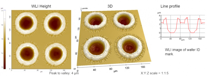
Scanning Conditions
- System : NX-Hybrid WLI
- Scan Mode: WLI
- Field of view: 182μm×182μm