-
Polyimide EFMAmplitude Flake Inorganic OrganicCompound Hafnia UTEM DomainSwitching UnivMaryland Adhesion MolecularSelfAssembly Korea Roughness PANI Granada LDPE Growing Magnetic Force Microscopy FAFailureAnlaysis Hydroxyapatite Mechinical India Neodymium Current Heating Tungsten HexagonalBN Boron SiWafer mechanical property Polymer CastIron VinylAlcohol Topography Electronics
Report image
If you found this image unacceptable, please let us know. We will review your report and take action if we determine this image is really unacceptable.
Semiconductor device, Failure analysis
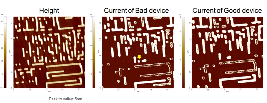
Scanning Conditions
- System: NX10
- Scan Mode: Conductive AFM
- Cantilever: CDT-Contr (k=0.5N/m, f=20kHz)
- Scan Size: 11μm×11μm
- Scan Rate: 1Hz
- Pixel: 512×512
- Sample bias: -0.5V