-
AM_SKPM IVSpectroscopy Phthalocyanine ChemicalCompound Heating blended polymers SetpointMode Co/Cr/Pt Polarization ThermalProperties I-VSpectroscopy nanomechanical Neodymium CompactDisk PolyvinylideneFluoride OpticalWaveguide Electrical&Electronics PVAC ferromagnetic Electrode PinPointMode Copper VinylAlcohol Tungsten_disulfide FastScan Fe_film Aluminium_Oxide Switching LMF Mechanical thermal_property Foil Polyaniline Conductivity SrO
Report image
If you found this image unacceptable, please let us know. We will review your report and take action if we determine this image is really unacceptable.
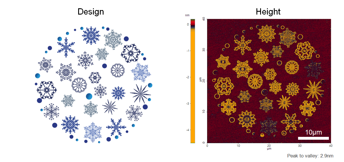
Christmas Ball Lithography on Si

Create oxidation layers on bare Si surface using bias mode of lithography.
Scanning Conditions
- System: NX10
- Scan Mode: Lithography
- Cantilever: AD-40-SS (k=40N/m, f=200kHz)
- Scan Size: 40μm×40μm
- Scan Rate: 0.5Hz
- Pixel Size: 1024 × 1024
- Tip Bias: -10V for patterened area
- Scan Mode: Lithography
- Cantilever: AD-40-SS (k=40N/m, f=200kHz)
- Scan Size: 40μm×40μm
- Scan Rate: 0.5Hz
- Pixel Size: 1024 × 1024
- Tip Bias: -10V for patterened area
