-
Silver Copolymer PVAP3HT TungstenDeposition Modulus Calcium temp Adhesion Polyethylene Insulator HexagonalBoronNitride KelvinProbeForceMicroscopy Battery TempControl YszSubstrate nanobar AM_KPFM LeakageCurrent Iron TemperatureControl Al2O3 Pinpoint ContactModeDot PolycrystallineFerroelectricBCZT Device TemperatureControllerAFM LateralForceMicroscopy Thermal IMT_Bucharest Strontium AmplitudeModulation Neodymium Metal-organicComplex GlassTemperature Polydimethylsiloxane
Report image
If you found this image unacceptable, please let us know. We will review your report and take action if we determine this image is really unacceptable.
MoS2 Layers on SiO2
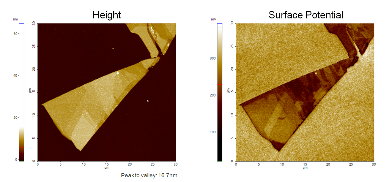
A few layers of MoS2 on SiO2
Scanning Conditions
- System: NX10
- Scan Mode: AM-KPFM
- Cantilever: NSC36Cr-Au B (k=2N/m, f=130kHz)
- Scan Size: 30μm×30μm
- Scan Rate: 0.3Hz
- Pixel Size: 512 × 256
- Scan Mode: AM-KPFM
- Cantilever: NSC36Cr-Au B (k=2N/m, f=130kHz)
- Scan Size: 30μm×30μm
- Scan Rate: 0.3Hz
- Pixel Size: 512 × 256