-
CeNSE_IISc fifber PatternedSapphireSubstrat LowDensityPolyethylene INSPParis graphene_hybrid Conduct InLiquid AmplitudeModulation LiquidCell Defect Solution Techcomp CP-AFM BoronNitride IIT-chennai Ni-FeAlloy Ni81Fe19 Leakage Filter plastics Zhi temp Battery PMNPT SicMosfet Sperm Epoxy Co/Cr/Pt food Beads ScanningThermalMicroscopy StrontiuTitanate MagneticPhase WPlug
Report image
If you found this image unacceptable, please let us know. We will review your report and take action if we determine this image is really unacceptable.
ITO Film Sputter Deposited onto Silicon
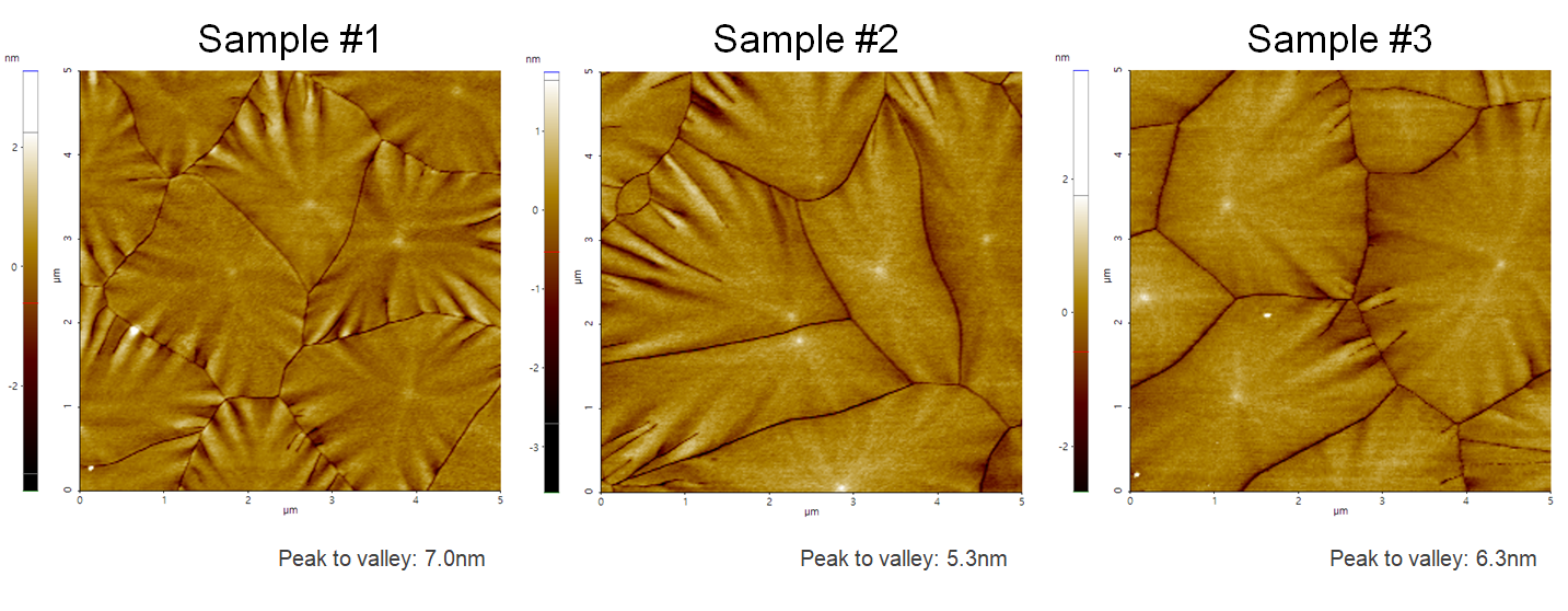
ITO-film, which was sputter deposited onto silicon. The grain size of those samples was influenced by changing the process settings in the Cluterline RAD sputter deposition system, one of the deposition tool platforms manufactured by Evatec.
Scanning Conditions
- System: NX10
- Scan Mode: Non-contact
- Cantilever: PPP-EFM (k=2.8N/m, f=75kHz)
- Scan Size: 5μm×5μm
- Scan Rate: 0.1Hz
- Pixel Size: 256 × 256
- Scan Mode: Non-contact
- Cantilever: PPP-EFM (k=2.8N/m, f=75kHz)
- Scan Size: 5μm×5μm
- Scan Rate: 0.1Hz
- Pixel Size: 256 × 256