-
fluorocarbon Ananth ImideMonomer Memory MultiLayerCeramicCapacitor LiquidCell temp Spain EPFL doped DeoxyribonucleicAcid Kevlar Au111 dichalcogenide StainlessSteel ForceDistanceSpectroscopy VortexCore SrO Epoxy KelvinProbeForceMicroscopy OpticalWaveguides Insulator semifluorinated_alkanes hetero_structure tip_bias_mode Mosfet UnivMaryland CompactDisk thermoplastic_elastomers BFO PVAP3HT SiWafer Sidewall InLiquid FAFailureAnlaysis
Report image
If you found this image unacceptable, please let us know. We will review your report and take action if we determine this image is really unacceptable.
MoS2 Layers on SiO2
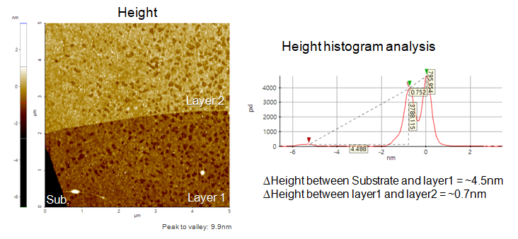
Scanning Conditions
- System: NX10
- Scan Mode: Non-contact
- Cantilever: AC160TS (k=26N/m, f=300kHz)
- Scan Size: 5μm×5μm
- Scan Rate: 1Hz
- Pixel Size: 256 × 256
- Scan Mode: Non-contact
- Cantilever: AC160TS (k=26N/m, f=300kHz)
- Scan Size: 5μm×5μm
- Scan Rate: 1Hz
- Pixel Size: 256 × 256