-
vertical_PFM ContactMode Boundary molecule Mosfet AAO ForceVolumeMapping DataStorage Subhajjit ItoGlass MolecularSelfAssembly Ram Battery Thermoplastic_polyurethane IISCBangalore Memory semifluorinated_alkanes StyreneBeads dielectric_trench biocompatible BariumTitanate Optoelectonics Display LiquidCrystal Melt organic_polymer Water lithography Regensburg Heating ChemicalCompound DiffractiveOpticalElements I-VSpectroscopy UnivOfMaryland EFMAmplitude
Report image
If you found this image unacceptable, please let us know. We will review your report and take action if we determine this image is really unacceptable.
Atomic steps on GaP(Gallium Phosphide) layer on Si
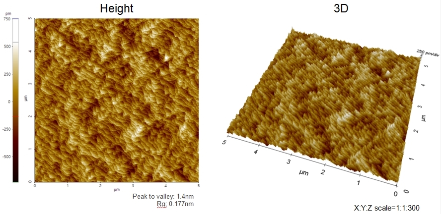
Scanning Conditions
- System: NX20
- Scan Mode: Non-contact
- Cantilever: PPP-NCHR (k=42N/m, f=300kHz)
- Scan Size: 5μm×5μm
- Scan Rate: 1Hz
- Pixel: 512×512