-
StrontiumTitanate Chrome VortexCore Hysteresys NUS Nanofiber Topography plastic Nanotechnology PUR piezoelectric force microscopy Potential Ceramics mono_layer ChemicalCompound Scratch hard_disk_media MechanicalProperties Pinpoint PolyvinylideneFluoride cannabis #EC PMNPT thermoplastic_elastomers Fendb pinpoint mode Hole ConductiveAFM Aluminum Gold OpticalModulator Leakage PhaseChange SKPM Celebration
Report image
If you found this image unacceptable, please let us know. We will review your report and take action if we determine this image is really unacceptable.
Photoresist pattern (post-development process)
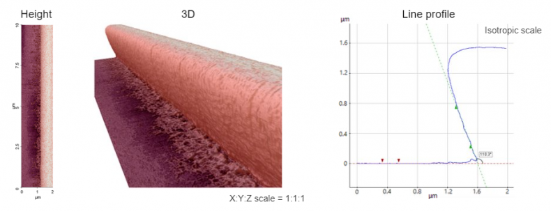
Scanning Conditions
- System : NX-3DM
- Scan Mode: Non-contact
- Scan Rate : 0.1 Hz
- Scan Size : 2μm×10μm
- Pixel Size : 512×2048
- Cantilever : EBD-R2-NCLR (k=45N/m, f=190kHz)