-
Terrace oxide_layer IVSpectroscopy Ananth Pores GranadaUniv LiftMode Protein Cobalt-dopedIronOxide plastics WS2 SAM Tungsten Materials Pinpoint HexagonalBoronNitride NUSNNI self-assembled_monolayer Transparent Sulfur mono_layer fifber Steps Biofilm PiezoelectricForceMicroscopy HydroGel Butterfly SPMLabs Forevision ThinFilm ContactModeDots Cell strontiu_titanate Composition Trench
Report image
If you found this image unacceptable, please let us know. We will review your report and take action if we determine this image is really unacceptable.
Chip
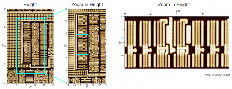
Scanning Conditions
- System : NX-Wafer
- Scan Mode: Non-contact
- Scan Rate : All 1Hz
- Scan Size : 25μm×40μm, 15μm×40μm, 8μm×4μm
- Pixel Size : 2048×256, 2048×256, 1024×256
- Cantilever : OMCL-AC160TS(k=26N/m, f=300kHz)