-
Alloy SiliconCrystal LogAmplifier neodymium_magnets ScanningIon-ConductanceMicroscopy StrontiuTitanate Korea InLiquid YttriaStabilizedZirconia SurfaceChange align Tungsten UnivCollegeLondon frequency_modulation NtuEee SolarCell mono_layer Blood Fendb Scratch silicon_carbide Growth contact HfO2 FAPbI3 HexagonalBoronNitride silicon_oxide tip_bias_mode temperature controller AFM biocompatible STO Polyethylene Gallium_Arsenide Hair BreastCancerCell
Report image
If you found this image unacceptable, please let us know. We will review your report and take action if we determine this image is really unacceptable.
WLI image of wafer ID mark
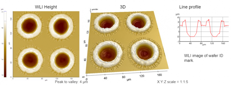
Scanning Conditions
- System : NX-Hybrid WLI
- Scan Mode: WLI
- Field of view: 182μm×182μm