-
MechanicalProperties Gallium_Arsenide Domain Bio WS2 InLiquid Non-ContactMode SicMosfet CalciumHydroxide StrontiuTitanate NanoLithography Laser Chloroform NCM Zagreb PatternedSapphireSubstrat Gong ThermalConductivity WWafer PrCurve Inorganic TyphimuriumBiofilm ferromagnetic Liquid ThinFilm Pores Polyurethane LowDensityPolyethylene Conduct Tungsten Yeditepe ConductingPolymer doped Metal-organicComplex LogAmplifier
Report image
If you found this image unacceptable, please let us know. We will review your report and take action if we determine this image is really unacceptable.
Monolayer Graphene on PDMS Surface
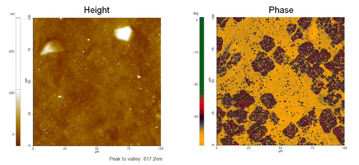
Monolayer Graphene grown on Cu foil using CVD process is transferred on to PDMS substrate.
Scanning Conditions
- System: NX20
- Scan Mode: Tapping
- Cantilever: Access-NC (k=113N/m, f=330kHz)
- Scan Size: 100μm×100μm
- Scan Rate: 0.6Hz
- Pixel Size: 256 × 256
- Scan Mode: Tapping
- Cantilever: Access-NC (k=113N/m, f=330kHz)
- Scan Size: 100μm×100μm
- Scan Rate: 0.6Hz
- Pixel Size: 256 × 256