-
Monisha FAPbI3 doped rubber Conduct FastScan Wang Holes Self-assembledMonolayer Workfunction Optic thermoplastic_elastomers HardDiskMedia Stiffness Photovoltaics Polyimide Writing organic_polymer CrystalGrowing Au111 Piezoelectric Neodymium CeNSE_IISc Chloroform layers exfoliate light_emission CP-AFM MagneticForceMicroscopy molecules MoS2 Liquid ElectroChemical Cross-section Christmas
Report image
If you found this image unacceptable, please let us know. We will review your report and take action if we determine this image is really unacceptable.
Fe Thin Films
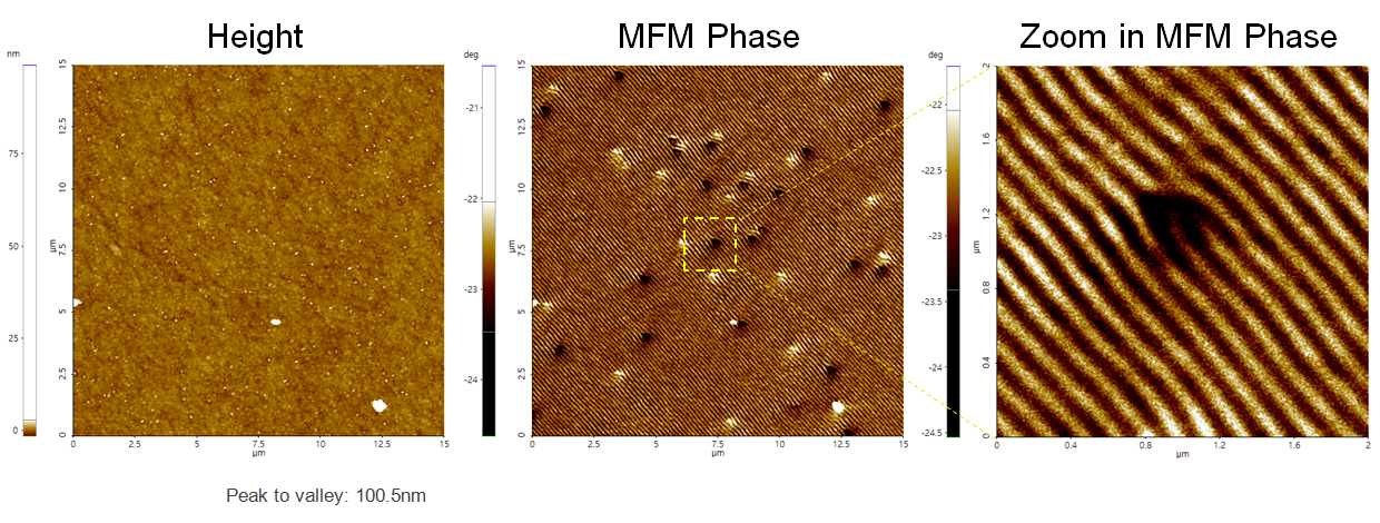
MFM images of Fe thin films (80 nm) epitaxied on GaAs(001) and then implanted with N-atoms. Images reveal weak stripe domains at magnetic remanence.
Scanning Conditions
- System: NX10
- Scan Mode: MFM
- Cantilever: PPP-MFMR (k=2.8N/m, f=75kHz)
- Scan Size: 15μm×15μm,2μm×2μm
- Scan Rate: 0.5Hz, 1Hz
- Pixel Size: 512×512, 256×256
- Lift height: 50nm
- Scan Mode: MFM
- Cantilever: PPP-MFMR (k=2.8N/m, f=75kHz)
- Scan Size: 15μm×15μm,2μm×2μm
- Scan Rate: 0.5Hz, 1Hz
- Pixel Size: 512×512, 256×256
- Lift height: 50nm