-
OpticalWaveguides YszSubstrate ferromagnetic Mosfet polymeric_arrays PtfeMembrane Dopped PvdfFilm Inorganic mechanical_property 2d_materials HighAspect Conductance BCZT C_AFM ito_film Sic PhaseImaging StainlessSteel ForceDistanceSpectroscopy thermal_conductivity Spain Polarization SICM LiNbO3 oxide_layer Kevlar Cell cannabinoid Ram Polyvinylidene Yeditepe_University Resistance Tapping HanyangUniv
Report image
If you found this image unacceptable, please let us know. We will review your report and take action if we determine this image is really unacceptable.
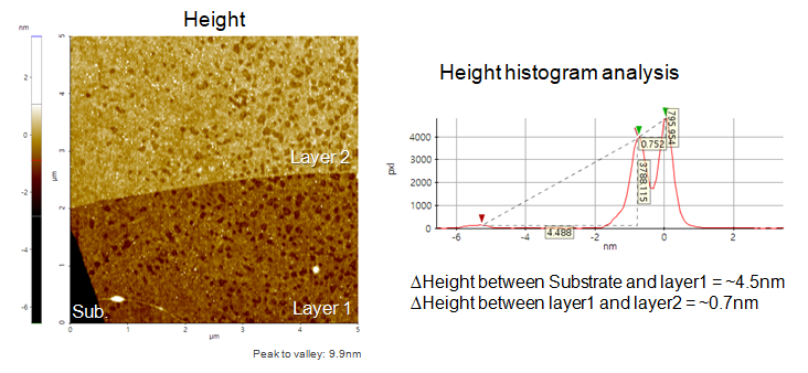
MoS2 Layers on SiO2
Scanning Conditions
- System: NX10
- Scan Mode: Non-contact
- Cantilever: AC160TS (k=26N/m, f=300kHz)
- Scan Size: 5μm×5μm
- Scan Rate: 1Hz
- Pixel Size: 256 × 256
- Scan Mode: Non-contact
- Cantilever: AC160TS (k=26N/m, f=300kHz)
- Scan Size: 5μm×5μm
- Scan Rate: 1Hz
- Pixel Size: 256 × 256