-
HexagonalBoronNitride BloodCell MoS2 Bismuth Mosfet Graphene dichalcogenide DataStorage Forevision Bio Pyroelectric CrystalGrowing Wafer NUS_Physics AtomicLayer Gold semifluorinated alkane CalciumHydroxide Hair Copolymer Electical&Electronics fluorocarbon GaP contact Composition Ceramic Dental block_copolymer StainlessSteel FloppyDisk molecular_self_assembly BaTiO3 blended polymers layers MagneticPhase
Report image
If you found this image unacceptable, please let us know. We will review your report and take action if we determine this image is really unacceptable.
Atomic steps on GaP(Gallium Phosphide) layer on Si
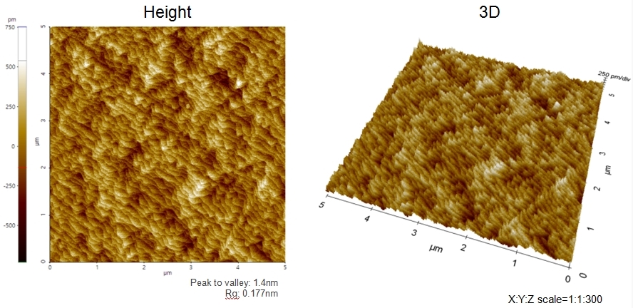
Scanning Conditions
- System: NX20
- Scan Mode: Non-contact
- Cantilever: PPP-NCHR (k=42N/m, f=300kHz)
- Scan Size: 5μm×5μm
- Scan Rate: 1Hz
- Pixel: 512×512