-
Alloy HanyangUniv Steps Dopped Magnetic PolymerPatterns Grain FAPbI3 LateralPFM P3HT Chemical_Vapor_Deposition EvatecAG Wafer DeoxyribonucleicAcid Oxide piezoelectric force microscopy Polystyrene PatternedSapphireSubstrat hetero_structure fluoroalkane CarbonNanotube PinPointMode SelfAssembly StainlessSteel PMNPT PinpointPFM OpticalModulator Phthalocyanine Corrosion FAFailureAnlaysis HafniumDioxide LifeScience Au111 ReflexLens ConductiveAFM
Report image
If you found this image unacceptable, please let us know. We will review your report and take action if we determine this image is really unacceptable.
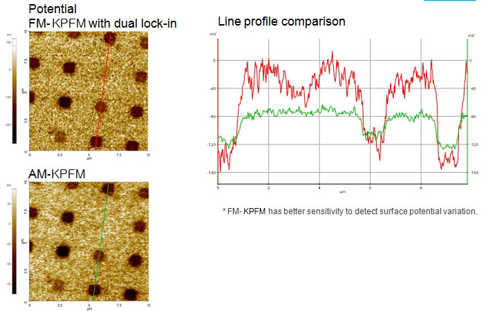
Polymer patterns on Si (2/2)
Scanning Conditions
- System: NX10
- Scan Mode: KPFM
- Cantilever: NSC36Cr-Au (k=1N/m, f=90kHz)
- Scan Size: 10μm×10μm
- Scan Rate: 0.2Hz
- Pixel: 512×256