-
hard_disk_media Grain MeltingPoint SurfaceOxidation silicon_oxide KelvinProbeForceMicroscopy AM_SKPM FM_KPFM Magnets FastScan Wafer Carbon Fiber ImideMonomer ForceMapping BariumTitanate Adhesive Korea LDPE ElectroChemical PANI Aggregated_molecules FM_SKPM KevlarFiber cannabis HafniumDioxide LiquidImaging frequency_modulation Conducting AAO PVAC Moire Implant PolymerBlend INSP
Report image
If you found this image unacceptable, please let us know. We will review your report and take action if we determine this image is really unacceptable.
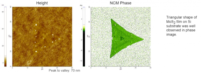
MoS₂ film

Scanning Conditions
- System : FX40
- Scan Mode: Tapping
- Scan Rate : 1Hz
- Scan Size : 40μm×40μm
- Pixel Size : 512×256
- Cantilever : OMCL-AC160TS (k=26N/m, f=300kHz)
