-
Hafnium_dioxide Phosphide Ferroelectric OxideLayer kelvin probe force microscopy ScanningThermalMicroscopy STO Tapping NusEce Barium_titanate Chrome Pore Korea LiquidCrystal Vac Transparent Techcomp self-assembled_monolayer Plug TungstenDeposition HBN Hexacontane semifluorinated alkane Electronics CP-AFM BCZT StrontiuTitanate Conductive AFM Molybdenum TemperatureControl ScanningSpreadingResistanceMicroscopy MagneticForceMicroscopy FM_KPFM silicon_oxide Holes
Report image
If you found this image unacceptable, please let us know. We will review your report and take action if we determine this image is really unacceptable.
GaN epi wafer
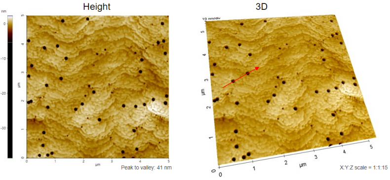
Scanning Conditions
- System : NX-Wafer
- Scan Mode: Non-contact
- Scan Rate : 0.7 Hz
- Scan Size : 5μm×5μm
- Pixel Size : 512×512
- Cantilever : PPP-NCHR (k=42N/m, f=330kHz)