-
Pinpoint fluoroaalkane TappingMode HanyangUniv medical lift_mode Ptfe Permalloy FloppyDisk PVAC TungstenThinFilmDeposition LowDensityPolyethylene PpLdpe OpticalModulator Varistor Metal-organicComplex MagneticForceMicroscopy non_contact CuParticle Hexacontane Molybdenum BiasMode sputter AnodizedAluminumOxide ThinFilm ChemicalCompound Grain Spincast nanomechanical Worcester_Polytechnic_Institute DeflectionOptics Piezoresponse AM_SKPM CastIron Graphite
Report image
If you found this image unacceptable, please let us know. We will review your report and take action if we determine this image is really unacceptable.
BN thin film on Si
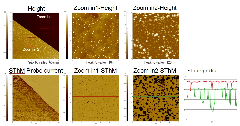
Scanning Conditions
- System: NX10
- Scan Mode:SThM
- Cantilever: Nanothermal probe
- Scan Size: 25μm×25μm, 5μm×5μm
- Scan Rate:0.3Hz, 0.5Hz
- Pixel: 256×256, 256×256
- Scan Mode:SThM
- Cantilever: Nanothermal probe
- Scan Size: 25μm×25μm, 5μm×5μm
- Scan Rate:0.3Hz, 0.5Hz
- Pixel: 256×256, 256×256