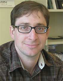
 Dr. Adam B. Braunschweig is an Assistant Professor in the Department of Chemistry at The University of Miami (FL). He received his B.A. in Chemistry from Cornell University (2001) and his Ph.D. in Organic Chemistry at the University of California-Los Angeles in 2006 with Prof. J.F Stoddart. He did post-doctoral research in nanotechnology at the Hebrew University of Jerusalem (Israel) with Professor Itamar Willner (2006-2007) and an NIH postdoctoral researcher in cancer nanotechnology with Professor Chad A. Mirkin at Northwestern University.
His recent honors include the NRSA Ruth L. Kirchstein postdoctoral fellowship from the NIH and an Air Force Office of Scientific Research (AFOSR) Young Investigator Award.
Areas of interest: nanolithography, organic chemistry, nanotechnology, materials science, organic photovoltaics, supramolecular chemistry.
Interview:
From a general perspective, Adam leads a research group that explores the interfaces of organic chemistry with biology and materials science to find new solutions to energy, health and environmental challenges.
Q: What are the fields of your research?
Some of the group’s research aims at improving the efficiency of photovoltaic (solar cell) technology. The potential for organic photovoltaics (OPVs) to improve on current silicon-based technology in cost and efficiency could be one of the most important contributions of technology in the 21st century. The group’s focus is on developing new materials for the active layers in organic photovoltaics in bulk heterojunction architectures.
Another area of research involves developing small molecules that can selectively bind carbohydrates, which could have applications in disease diagnosis, drug delivery and as therapy.
The third area of research is nanolithography. We are trying to improve on the techniques of softlithography and dip-pen nanolithography (DPN). We’ve turned to Polymer Pen Lithography (PPL) and Hard Tip, Soft Spring Lithography (HSL) that can be performed in massively parallel arrays with edge lengths between 80 nm and 10 micrometers.
Q: Can you tell us about the studies you are doing using an AFM?
We use AFM in all three of our research areas. Most frequently, we use AFM in nanolithography. Specifically, a Park Systems XE 150 system is crucial to create controllable surface patterns of carbohydrate molecules. We also routinely use contact and non-contact AFM techniques for imaging bulk heterojunction active layers in photovoltaics.
Q: What made AFM the best choice for your study?
With regard to the lithography, it’s very difficult to create sub-micrometer feature sizes of soft matter. There is ink jet or pin printing but the length scale of those features is typically on the order of 100 microns. So with regard to small feature sizes, there is soft lithography but it is limited to patterns that are dictated by the structure of a predetermined master that is created by conventional silicon microfabrication. The AFM with computer-controlled actuation gives us much more flexibility in the patterns we can create. I can say there really isn’t a good alternative technology for this.
Q: How well is Park AFM meeting your research needs?
Park is a great company to work with. Here’s an example: When we came up with the idea of polymer pen lithography, I went to all the major AFM companies to see what they could offer. Park had the best system and was also the most willing to work with us. I’ve been involved in purchase of five of these things (Park XE-150 systems), which I think shows how satisfied I am with the results.
Q: What are the key features of Park AFM that you like the most?
For some of our work, especially nanolithography, we have a customized platform. I really liked the way Park worked with me to make the platform adaptations I requested. Oh, and it doesn’t break down – which I really like.
Changing the scanning head is easy to do for different modes. I think the Park equipment is pretty easy. I need students to use the equipment – frequently – and I don’t like instruments that require a Ph.D. to figure out how to use them.
Q: What is more important to you, accuracy (vs.) resolution (vs.) scan speed?
For us, the scan speed is important; we’re less concerned about stuff like XY resolution since we deal mostly with things in the 100-150 nm range where noise is not much of an issue. Also, ease of use is very important to us, especially the software. In general, with Park microscopes the speed of the machine exceeds what we need.
Recent Published Work Using Park AFM: Title: Matrix-assisted polymer pen lithography induced Staudinger Ligation
Author(s): Shudan Bian, Keving B. Schesing and Adam B. Braunschweig
Source: Chem. Comm., 2012, 48 Pages: 4995-4997 DOI: 10.1039/c2cc31615c
Title: Polymer Pen Lithography (PPL)-Induced Site-Specific Click Chemistry for the Formation of Functional Glycan Arrays
Author(s): Shudan Bian, Jiajun He, Kevin B. Schesing, and Adam B. Braunschweig
Source: wileyonlinelibrary.com Volume: 8 Issue: 13 Pages: 2000-2005 DOI: 10.1002/smll.201102707 Published: April 10, 2012 small 2012
