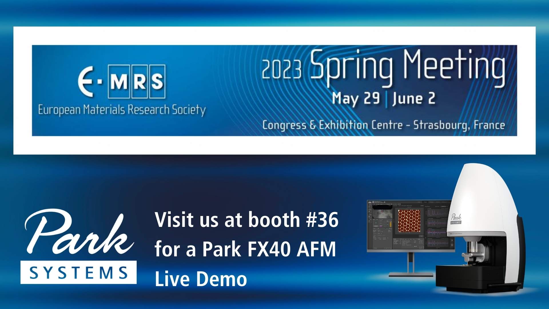
The European Materials Research Society will be celebrating it’s 40-year anniversary at the 2023 E-MRS Spring Meeting and Exhibit from May 29 to June 2, 2023 at the Convention & Exhibition Centre of Strasbourg (France). Park Systems is proud to be a part of this celebration and join the event as an exhibitor and speaker!
With numerous symposiums and plenary sessions E-MRS Spring Meeting provides a forum to discuss current trends and cutting-edge research on nanomaterials, biomaterials and nanomedicine, semiconductors and nanodevices, material processing and characterization setting up trends and future paths in material research field.
Step by Park’s booth #36 to discuss with us the automation of nanoscale imaging process on the #FX40 Automatic AFM and its advantages for investigating materials at nanoranges! Don’t wait and book a demo slot today: pse.sales@parksystems.com
- • Time: May 29 – June 2, 2023 (Exhibition from May 30 – June 1)
- • Venue: Palais de la Musique et des Congrès, Palace de Bordeaux, 67082 Strasbourg, France
- • Our location: booth #36
On top of that, we will be presenting a talk on “Probing the electrical properties of graphene and hexagonal boron nitride multi-layers at nanoscale via Scanning Probe Microscopy techniques".
When: Tuesday 30th of May at 1.30 pm - session E04 - ref. 02174 in symposium E. "Carbon- and/or nitrogen-containing thin films and nanomaterials”.
________________________________________________________________________________________________________

Join Dr. Alexander Klasen, Principal Scientist at Park Systems Europe at E-MRS 2023 for his talk:
- ⏩ TALK: “Probing the electrical properties of graphene and hexagonal boron nitride multi-layers at nanoscale via Scanning Probe Microscopy techniques”
- ⏩ DATE: Tuesday 30th of May at 1.30 pm - session E04 - ref. 02174 in symposium E. "Carbon- and/or nitrogen-containing thin films and nanomaterials”
Abstract:
Presenting Author: Alexander Klasen¹
Co-Author: Andrea Cerreta¹
¹Park Systems Europe GmbH, Schildkrötstraße 15, Mannheim, Germany
In an ever-advancing miniaturization of our modern, high-tech world, thin films and multi-layered materials gain increasing attention as they could pave the way to novel applications like ultra-thin ferroelectrics, protective coatings with adjustable friction, or tailored conductive properties [1-3]. In this sense, the thinnest films imaginable are single layers of 2D materials like graphene, hexagonal boron nitride (hBN), or transition metal dichalcogenides (TMDs) like (tungsten disulfide) WS2. However, reliable application of such nanometer-sized structures requires a correlative metrology that resolves such features [4].
Here, atomic force microscopy (AFM) has been established as a most versatile tool for the characterization of structures and interfaces with sub-nanometer resolution. The unique utilization of a nanometric probe in close proximity to the sample allows for a series of advanced characterizations of the material properties beyond crucial topographical information such as step height, roughness, and lattice periodicity. Nanomechanical measurements to map the adhesion, stiffness, or even friction with unparalleled high resolution can be performed. The ability to apply a bias locally permits to correlate these properties with additional features like the work function and conductance. This provides a comprehensive investigation of morphology and defects with a broad spectrum of local information, which helps to optimize the preparation and development of new materials. Lastly, a high degree of automation enables AFM systems to program batch processes for wafer sampling, e.g. to study sample degradation vs. time caused by various factors, including illumination or humidity.
In this talk, we demonstrate the versatility of AFM via a nanoscale characterization and manipulation of switchable ferroelectric domains in hBN/graphene heterostructures. Moreover, we assess the correlation between the presence of defects on graphene coatings and the variation of the local surface potential. Finally, we show how scanning probe electrochemical experiments are able to correlate surface reactivity with the chemical composition and arrangement of multi-layers.
- [1] N. R. Glavin et al., Adv. Mater. 32. 7 (2020) 1904302
- [2] A. Gupta et al., Progress in Materials Science 73 (2015) 44-126
- [3] C. Cui et al., NPJ 2D Materials and Applications 2 (2018) 18
- [4] M. Vizner Stern et al., Science 372, 6549 (2021) 1462-1466
________________________________________________________________________________________________________
About the European Materials Research Society:
E-MRS now has more than 4,000 members from industry, government, academia and research laboratories, who meet regularly to debate recent technological developments of functional materials. The E-MRS differs from many single-discipline professional societies by encouraging scientists, engineers and research managers to exchange information on an interdisciplinary platform, and by recognizing professional and technical excellence by promoting awards for achievement from student to senior scientist level. As an adhering body of the International Union of Materials Research Societies (IUMRS), the E-MRS enjoys and benefits from very close relationships with other Materials Research organizations elsewhere in Europe and around the world.
Link: https://www.european-mrs.com/meetings/2023-spring-meeting
